Selective solder mask printing on a printed circuit board (PCB)

a printed circuit board and solder mask technology, applied in the direction of printing, printed circuit manufacture, electrical equipment, etc., can solve the problems of waste of time and human resources, production requires additional work, and the electrical circuit is not working normally

Active Publication Date: 2016-09-29
CAMTEK LTD
View PDF3 Cites 2 Cited by
  • Summary
  • Abstract
  • Description
  • Claims
  • Application Information

AI Technical Summary

Benefits of technology

[0019]The printing of the first ink on the object at locations that correspond to the actual locations of the substrate holes may exhibit a first printing speed; wherein the printing of the second ink on the substrate thereby forming the predefined pattern on the substrate may exhibit a second printing speed that may be lower than the first printing speed.

Problems solved by technology

Currently in regular process of electrical circuits manufacturing such as PCB, non-conductive layer (such as Solder Mask for example) cannot be applied till the edge of the drill holes or Through silicon vias (TSV-s) or other holes in the substrate due to the fact that it blocks the hole and creates an air bubbles in the hole—this air bubble can explode in the process of soldering that leads to malfunction of the electrical circuit and wastage of the material.
The current solution of the problem is to clog the holes with the clogging material and applying the solder mask over the clogged holes—this way of production requires an additional work and waste of time and human resources.

Method used


Image

  • Selective solder mask printing on a printed circuit board (PCB)
  • Selective solder mask printing on a printed circuit board (PCB)
  • Selective solder mask printing on a printed circuit board (PCB)

Examples


Embodiment Construction

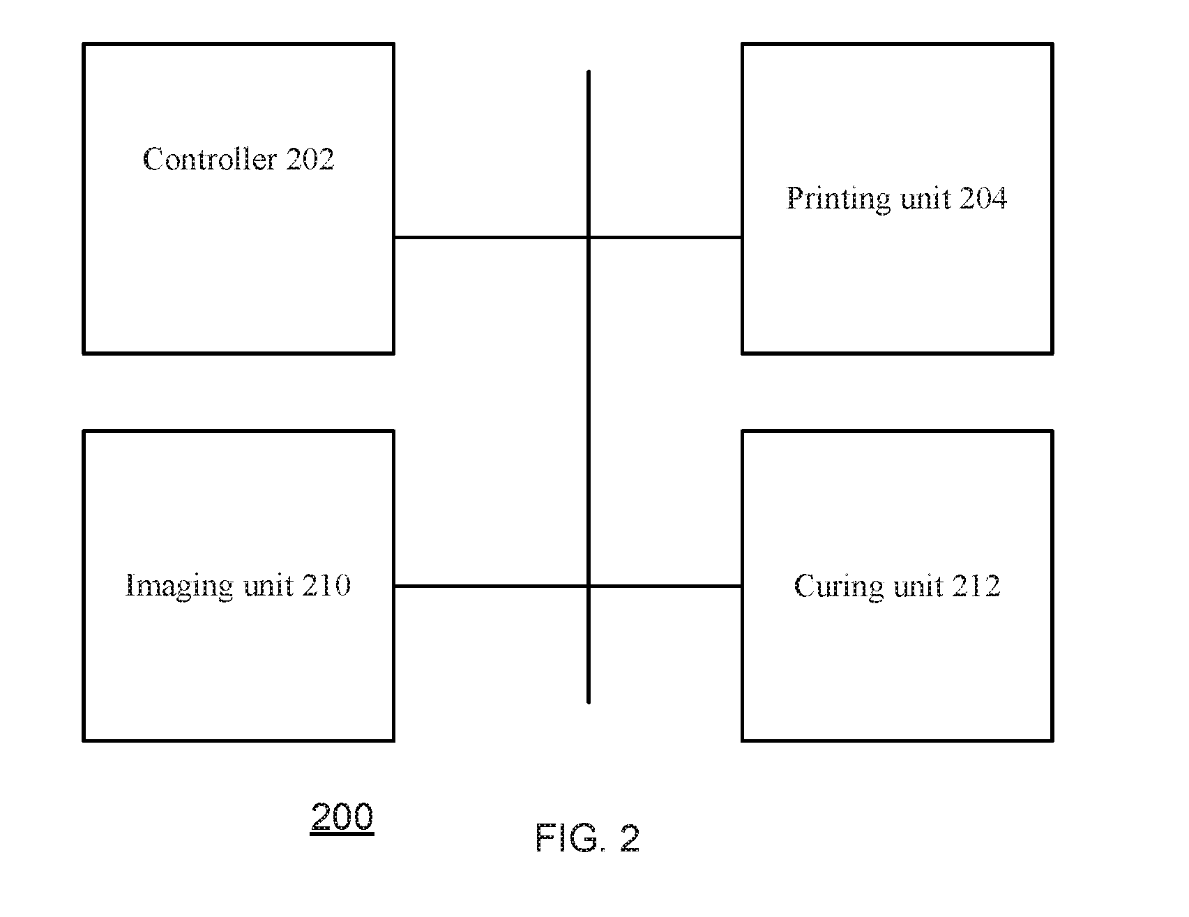
[0026]Because the apparatus implementing the present invention is, for the most part, composed of electronic components and circuits known to those skilled in the art, circuit details will not be explained in any greater extent than that considered necessary as illustrated above, for the understanding and appreciation of the underlying concepts of the present invention and in order not to obfuscate or distract from the teachings of the present invention.

[0027]In the following specification, the invention will be described with reference to specific examples of embodiments of the invention. It will, however, be evident that various modifications and changes may be made therein without departing from the broader spirit and scope of the invention as set forth in the appended claims.

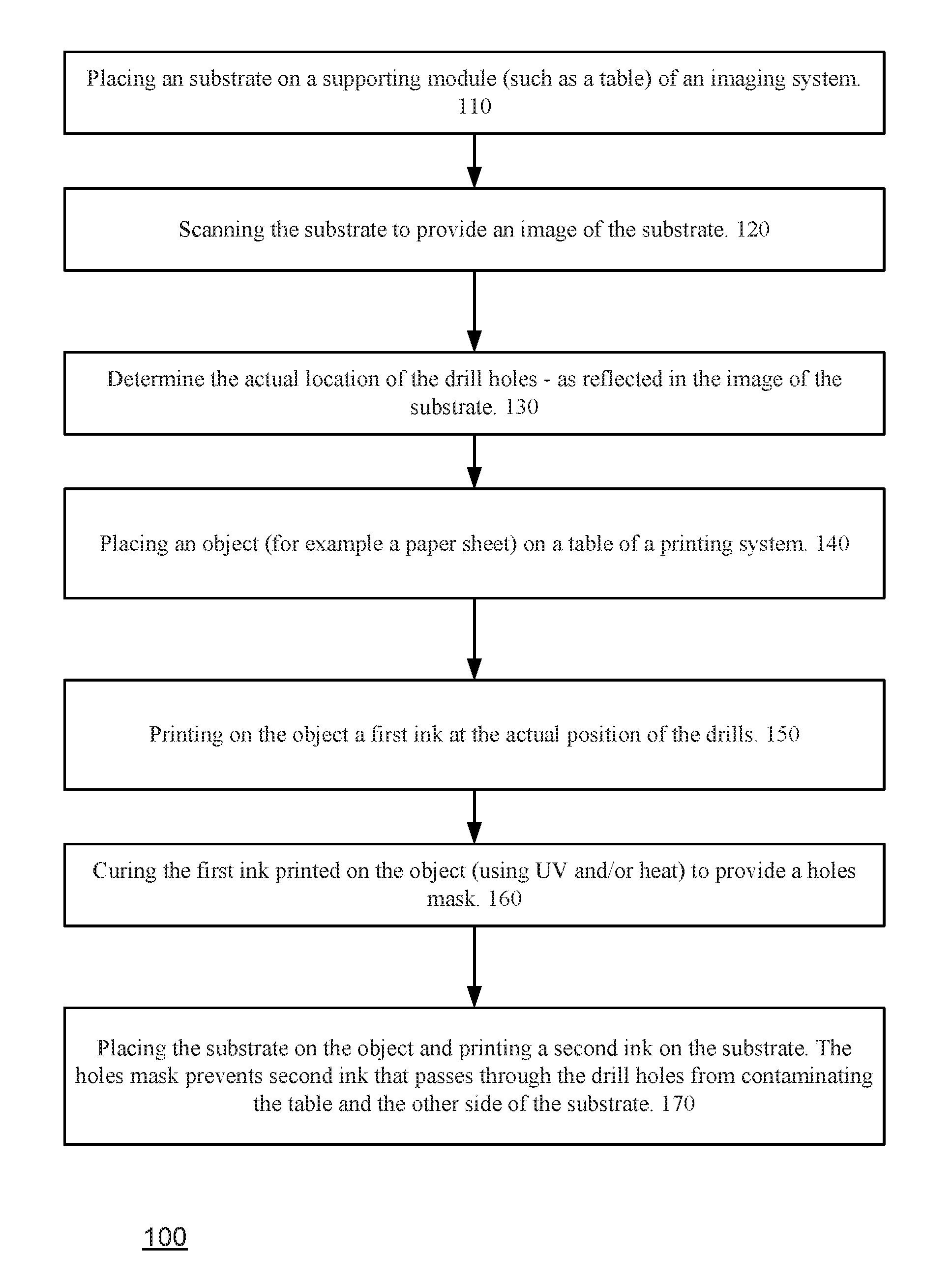
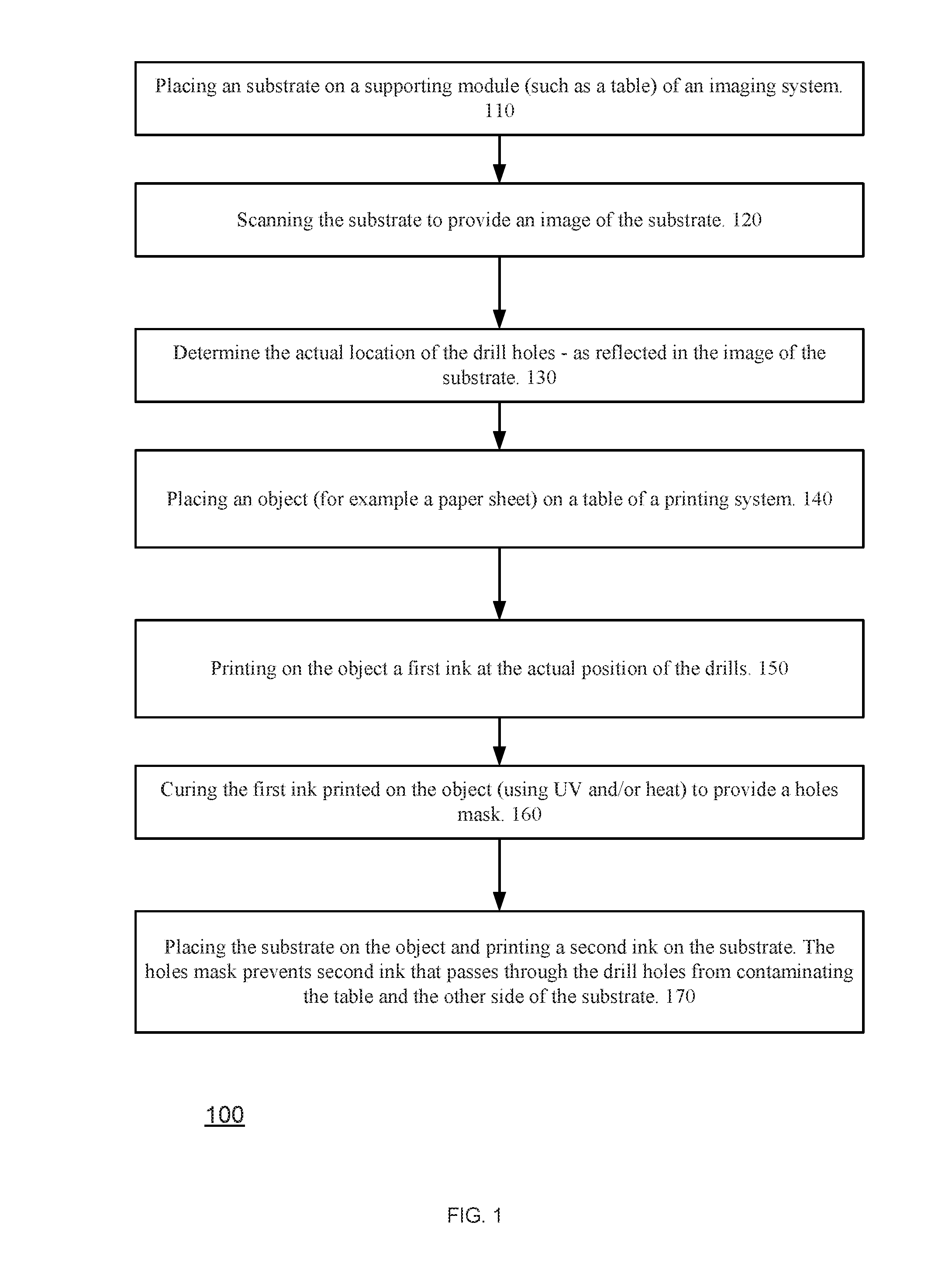
[0028]The method allows to print non-conductive layer (such as printing Solder Mask) till the edge of the hole (of the drill or TSV or any other type) without contaminating the other side of the substrate an...


PUM


Abstract

A method for printing on a substrate, the method may include determining actual locations of substrate holes; printing a first ink on an object at locations that correspond to the actual locations of the substrate holes and curing the first ink to provide a holes mask; and wherein after the substrate is positioned on the object so that holes mask seals bottoms of the substrate holes then printing the second ink on the substrate thereby forming a predefined pattern on the substrate.

Description

CROSS REFERENCE TO RELATED APPLICATIONS[0001]This patent application claims the priority of U.S. provisional patent Ser. No. 62 / 137,841 filed Mar. 25, 2015, which is incorporated herein by reference.BACKGROUND OF THE INVENTION[0002]Currently in regular process of electrical circuits manufacturing such as PCB, non-conductive layer (such as Solder Mask for example) cannot be applied till the edge of the drill holes or Through silicon vias (TSV-s) or other holes in the substrate due to the fact that it blocks the hole and creates an air bubbles in the hole—this air bubble can explode in the process of soldering that leads to malfunction of the electrical circuit and wastage of the material. The current solution of the problem is to clog the holes with the clogging material and applying the solder mask over the clogged holes—this way of production requires an additional work and waste of time and human resources.SUMMARY OF THE INVENTION[0003]According to an embodiment of the invention t...

Claims


Application Information

Patent Timeline
Patent Type & Authority Applications(United States)
IPC IPC(8): H05K3/00B41J3/407
CPCB41J3/407H05K3/0079B41J2/01H05K1/0269H05K3/0094H05K3/3452H05K2203/013H05K2203/1476H05K2203/166H05K3/0073
Inventor BEN-ABU, YEHUDAOZERI, YAIR
Owner CAMTEK LTD
Why Eureka
Try Eureka