Spin Transfer MRAM Device with Reduced Coefficient of MTJ Resistance Variation

a technology of mtj resistance variation and spin transfer mram, which is applied in the direction of information storage, static storage, digital storage, etc., can solve the problems of increasing power consumption, affecting the operation of the device, so as to increase the read margin

Active Publication Date: 2016-11-10
TAIWAN SEMICON MFG CO LTD
View PDF4 Cites 5 Cited by
  • Summary
  • Abstract
  • Description
  • Claims
  • Application Information

AI Technical Summary

Benefits of technology

[0021]A first object of this invention is to provide an MRAM device configuration that provides a greatly increased read margin while not requiring any increase in critical current or local transistor size.

Problems solved by technology

The use of magnetic fields externally generated by current carrying lines (as in FIG. 1) to switch the magnetic moment directions becomes problematic as the size of the MRAM cells decreases and, along with their decrease, so does the width of the current carrying lines.
The smaller width lines require greater current densities to produce the necessary switching fields on the MTJ elements, greatly increasing power consumption.
It is to be noted that large cell arrays are subject to difficulties that arise from statistical variations in the magnetic and electrical properties of each cell.
However, statistical variations in the high and low resistance values of the array cells and the reference cells often make it possible to incorrectly interpret the resistance value of a cell.
This high current density, which is required to induce the spin transfer effect, could destroy the insulating tunneling barrier in the MTJ cell, such as a layer of AlOx, MgO, etc.
This makes the reading process very difficult, even impossible, without a great increase in the magneto-resistive ratio dR / R.
None of the above prior art discuss a method for reducing resistance variation, which will help the reading process for a spin-transfer MRAM.

Method used


Image

  • Spin Transfer MRAM Device with Reduced Coefficient of MTJ Resistance Variation
  • Spin Transfer MRAM Device with Reduced Coefficient of MTJ Resistance Variation
  • Spin Transfer MRAM Device with Reduced Coefficient of MTJ Resistance Variation

Examples


first embodiment

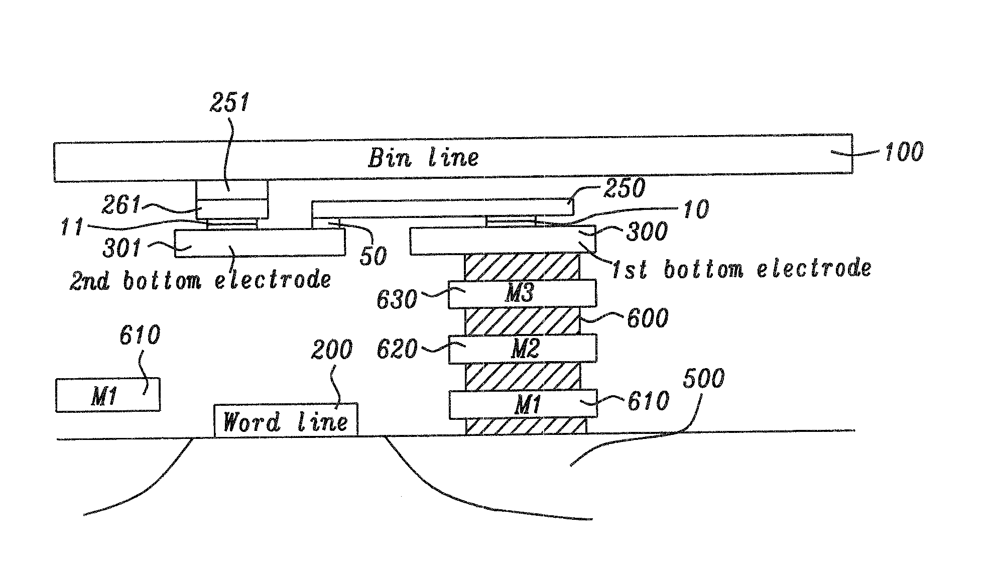
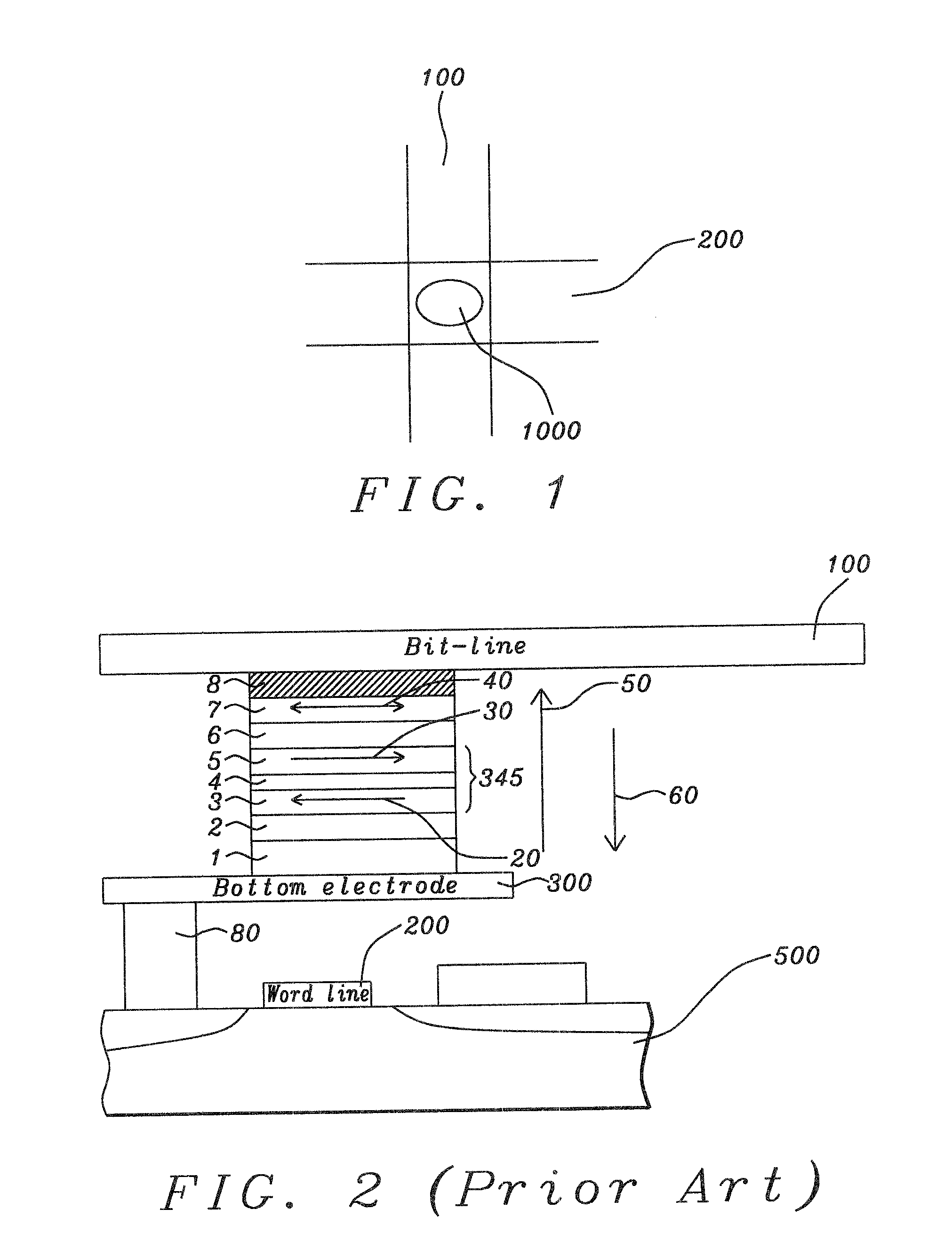
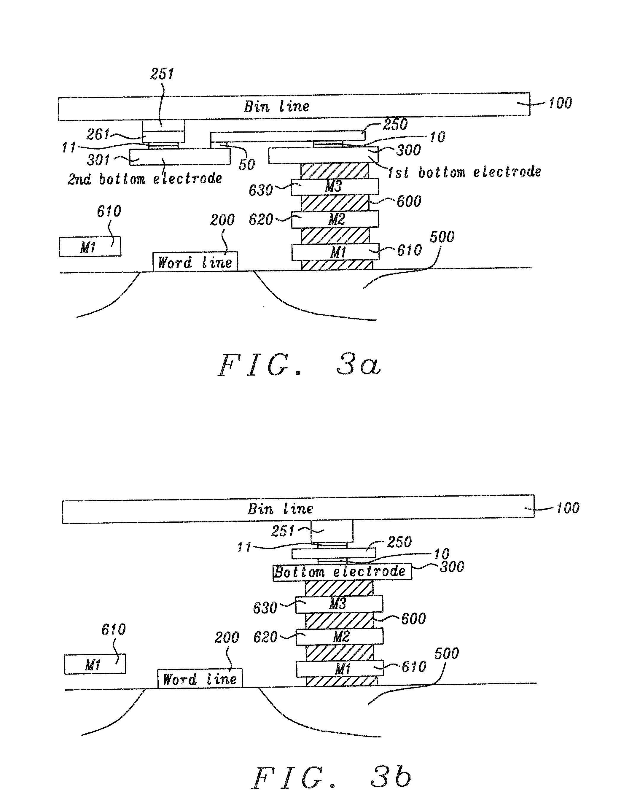
[0030]Referring to FIG. 3a, there is shown this invention. In this embodiment a plurality of N sub-cells, where N is an integer greater than 1 (only two (10), (11) being shown for simplicity) are formed in a horizontal series connected sequence. Looking downward from the top of the diagram, there is shown a horizontally extending bit line (100). At the bottom of the diagram is shown (highly schematically) a current providing transistor (500). A word line (200) that extends perpendicularly to the plane of the figure and, correspondingly, transverse to the bit line, substantially contacts the gate of the transistor. A conducting via (600) is shown extending upward through three exemplary layers (610), (620), (630) of metallization (levels of the circuit integration along which electrical connections are made) to ultimately contact the bottom electrode (300) of a first MTJ sub-cell (10). The first sub-cell has a top electrode (250) which extends horizontally to electrically contact the...

second embodiment

[0032]Referring now to FIG. 4a, there is shown, schematically, a typical fabrication process of this second embodiment, in which the sub-cells are series connected in a vertical configuration. In this process there is first formed on a substrate (1000) a first bottom electrode (300) on which is formed a first MTJ element film stack (10) that will subsequently be patterned to become the first sub-cell. The substrate may already contain a conducting via (600) that connects to a transistor in a lower layer of the fabrication. This via will not be shown in subsequent drawings but its presence is understood. Note, in this terminology the film stack refers to the succession of vertically stacked layers that, when horizontally patterned, will become an MTJ sub-cell. The vertical structure of the stack is the same as the vertical structure of the MTJ cell shown in FIG. 2, so, for clarity, the stack will be shown as a layer (10) without structure.

[0033]The horizontal extent of the film stack...


PUM


Abstract

We describe the manufacturing process for and structure of a CPP MTJ MRAM unit cell that utilizes transfer of spin angular momentum as a mechanism for changing the magnetic moment direction of a free layer. The cell is formed of a vertically or horizontally series connected sequence of N sub-cells, each sub-cell being an identical MTJ element. A statistical population of such multiple sub-cell unit cells has a variation of resistance that is less by a factor of N−1 / 2 than that of a population of single sub-cells. As a result, such unit cells have an improved read margin while not requiring an increase in the critical switching current.

Description

BACKGROUND OF THE INVENTION[0001]1. Field of the Invention[0002]This invention relates generally to a current perpendicular to plane random access memory (CPP-MRAM) cell formed as a magnetic tunneling junction (MTJ) and using a spin transfer effect with enhanced spin torque.[0003]2. Description of the Related Art[0004]The conventional magnetic tunneling junction (MTJ) device is a form of ultra-high magnetoresistive device in which the relative orientation of the magnetic moments of parallel, vertically separated, upper and lower magnetized layers controls the flow of spin-polarized electrons tunneling through a very thin dielectric layer (the tunneling barrier layer) formed between those layers. When injected electrons pass through the upper layer they are spin polarized by interaction with the magnetic moment of that layer. The majority of the electrons emerge polarized in the direction of the magnetic moment of the upper layer, the minority being polarized opposite to that directi...

Claims


Application Information

Patent Timeline
Patent Type & Authority Applications(United States)
IPC IPC(8): G11C11/16
CPCG11C11/161G11C11/1655G11C11/1657G11C11/1659G11C11/1673G11C11/1675G11C11/16
Inventor GUO, YIMIN
Owner TAIWAN SEMICON MFG CO LTD
Why Eureka
Try Eureka