Array substrate, liquid crystal panel and liquid crystal display device

Active Publication Date: 2016-11-17
TCL CHINA STAR OPTOELECTRONICS TECH CO LTD
View PDF0 Cites 6 Cited by
  • Summary
  • Abstract
  • Description
  • Claims
  • Application Information

AI Technical Summary

Benefits of technology

The invention provides an array substrate with improved design for connection between sub-pixels and data lines / scan lines. This design results in better improvement of bright and dark vertical lines in a liquid crystal panel, by balancing the charging of sub-pixels and reducing the effect of poorly-charged sub-pixels. Overall, the invention provides a more uniform and improved display with improved image quality.

Problems solved by technology

Since the data line has a certain resistance, the data signal would have the delay and distortion of waveform during transmission on the data line, resulting in a charging ratio difference of sub-pixels in adjacent columns of the data line.
However, in one signal polarity period, owing to the signal distortion, the previously charged sub-pixels P12, P22 are insufficiently / poorly charged and thus have a relatively low brightness, and the latterly charged sub-pixels P13, P23 are well charged and thus have a relatively high brightness, so that significant bright and dark lines are generated.

Method used


Image

  • Array substrate, liquid crystal panel and liquid crystal display device
  • Array substrate, liquid crystal panel and liquid crystal display device
  • Array substrate, liquid crystal panel and liquid crystal display device

Examples


embodiment 1

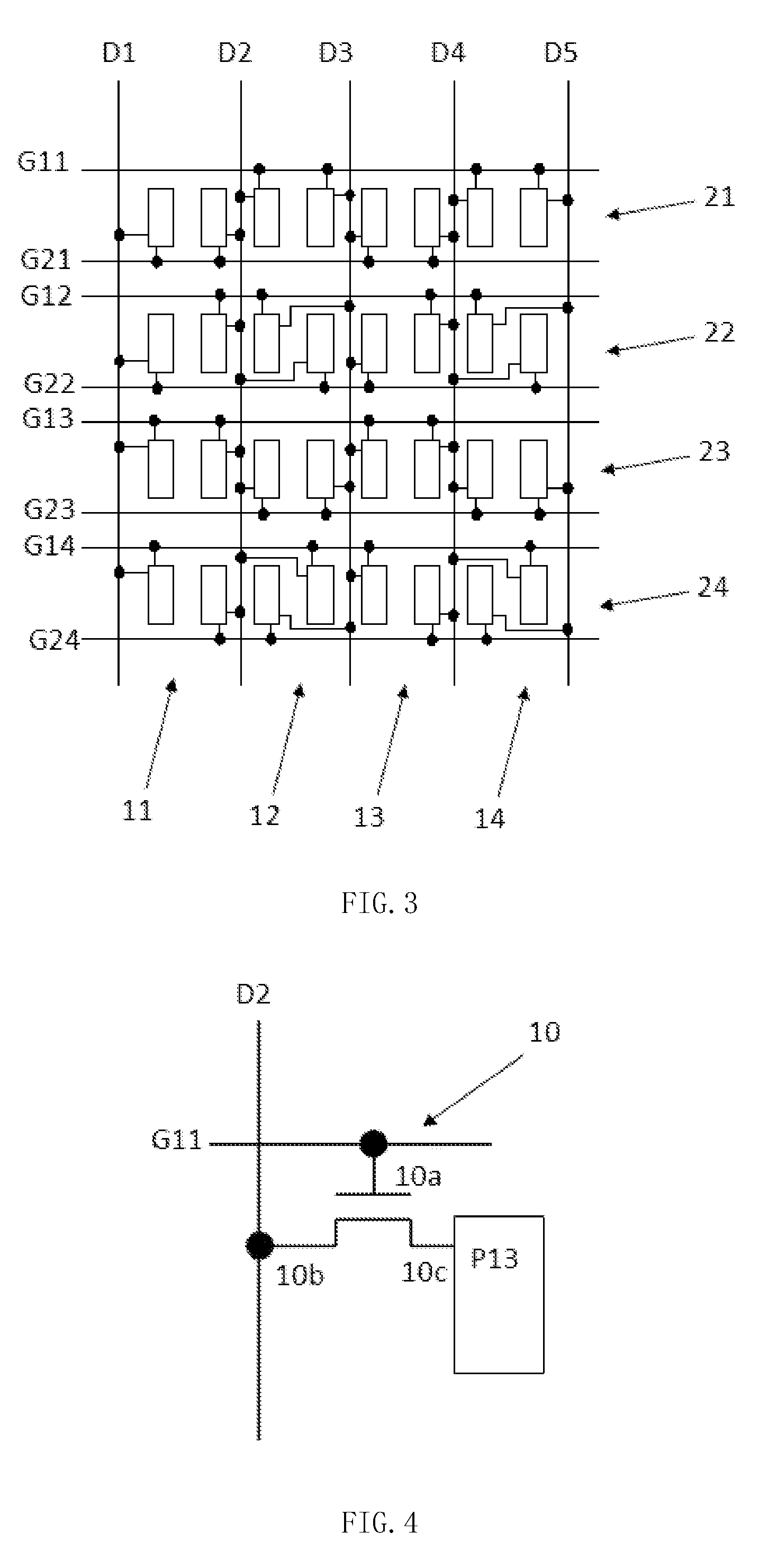
[0045]FIG. 3 is a schematic partial structural view of an array substrate provided by this embodiment. Hereinafter, Pxy represent specific sub-pixels, where x=1˜4, y=1˜8. For example, in FIG. 3, P11 is the first sub-pixel at the top-left corner, and P48 is the last sub-pixel at the bottom-right corner.

[0046]As shown in FIG. 3, in data lines D1˜D5, each two data lines define a corresponding one of column groups 11, 12, 13, 14 arranged therebetween, and each column group includes two columns of sub-pixels, e.g., the column group 11 in FIG. 3 includes the first and the second columns of sub-pixels.

[0047]In particular, for the sub-pixels in the odd column groups 11, 13, each sub-pixel is connected to one of the two data lines at two sides of the column group which is closer to the sub-pixel, e.g., for the sub-pixels in the column group 11, the sub-pixels P1y are connected to the data line D1, and the sub-pixels P2y are connected to the data line D2. For the sub-pixels in odd rows of the...

embodiment 2

[0057]FIG. 6 is a schematic partial structural view of an array substrate provided by this embodiment. What is difference from the embodiment 1 is that: in this embodiment, along the arrangement direction of the scan lines, the sub-pixel array is divided into row groups 21a, 22a, 23a, 24a, each row group includes two rows of sub-pixels. Specifically, as illustrated in FIG. 6, the row group 21a includes the first and the second rows of sub-pixels, the row group 22a includes the third and the fourth rows of sub-pixels, the row group 23a includes the fifth and the sixth rows of sub-pixels, and the row group 24a includes the seventh and the eighth rows of sub-pixels.

[0058]A connection manner of one row of sub-pixels in each row group with data lines and scan lines is the same as a connection manner of the other one row of sub-pixels in the row group with data lines and scan lines, that is, two rows of sub-pixels are used as one repeating unit. For example, in the row group 21a, for all ...

embodiment 3

[0060]Referring to FIG. 8 and FIG. 9, this embodiment provides a liquid crystal panel and a liquid crystal display device including the liquid crystal panel. As illustrated in FIG. 8, the liquid crystal display device includes a liquid crystal panel 100 and a backlight module 200. The liquid crystal panel 100 and the backlight module 200 are oppositely disposed. The backlight module 200 is configured (i.e., structured and arranged) for providing a display light source for the liquid crystal panel 100 and thereby facilitating the liquid crystal panel 100 to display an image.

[0061]As illustrated in FIG. 9, the liquid crystal panel 100 includes a display unit 1 formed with an array of sub-pixels, a gate driver 2 and a source driver 3. The gate driver 2 is configured for supplying scan signals Gate to the array of sub-pixels through scan lines, and the source driver 3 is configured for supplying data signals Data to the array of sub-pixels through data lines.

[0062]FIG. 10 is a schematic...


PUM


Abstract

The invention provides an array substrate including an array of sub-pixels, multiple data lines and multiple scan lines. The array of sub-pixels is divided into multiple column groups along the arrangement direction of the data lines and divided into multiple row groups along the arrangement direction of the scan lines. By the arrangement design of a connection manner of the sub-pixels with the data lines and scan lines in the array substrate, when is driven by a dot inversion method, each column of sub-pixels have intervally arranged well-charged sub-pixels and poorly-charged sub-pixels, so that in a liquid crystal panel including the array substrate, brightnesses of various areas are balanced on the whole and the drawback of the existence of bright and dark lines in the vertical direction is improved. A liquid crystal panel including the array substrate, and a corresponding liquid crystal display device also are provided.

Description

TECHNICAL FIELD[0001]The present invention relates to the field of liquid crystal display technology, and particularly to an array substrate, a liquid crystal panel and a liquid crystal display device.DESCRIPTION OF RELATED ART[0002]The liquid crystal display (LCD) device is a type of an ultrathin flat display device, and the liquid crystal panel is an important part of the liquid crystal display device. Generally, the liquid crystal panel at least includes oppositely-disposed array substrate and color filter substrate and a liquid crystal layer arranged between the array substrate and the color filter substrate. The array substrate is formed with a pixel array and mutually intersected data lines and scan lines. The data lines are configured to supply data signals to the pixel array, and the scan lines are configured to supply scan signals to the pixel array. In a traditional array substrate, pixels in a same column are connected to a same data line and thereby the data line is resp...

Claims


Application Information

Patent Timeline
IPC IPC(8): G02F1/1362G02F1/1335G02F1/1368
CPCG02F1/136286G02F1/133514G02F1/1368H01L27/124G09G3/3648G09G2300/0426G09G2310/0218G09G2310/0283G02F1/1362G09G3/3607G09G3/364
Inventor LI, QIANQIANHSU, JE-HAOCHEN, CAIQIN
Owner TCL CHINA STAR OPTOELECTRONICS TECH CO LTD
Why Eureka
Try Eureka