Packaging module and substrate structure thereof

a technology of packaging modules and substrates, applied in the field of substrate structures, can solve the problems of adversely affecting the quality of conductive through holes, the overall fabrication cost of the substrate structure b>1/b>′ is increased, etc., and achieves the effects of reducing the number of layers of the wiring portion, reducing the fabrication cost, and low cos

Active Publication Date: 2017-02-16
PHOENIX PIONEER TECH
View PDF2 Cites 6 Cited by
  • Summary
  • Abstract
  • Description
  • Claims
  • Application Information

AI Technical Summary

Benefits of technology

[0024]According to the present disclosure, a circuit board is fabricated first and then introduced into a general substrate process. As such, a high-cost insulating material is only applied in the circuit board, and the first insulating layer can be made of a low-cost material. Compared with the prior art, the substrate structure according to the present disclosure has a lower fabrication cost.
[0025]Further, fine-pitch circuits are formed in the circuit board, and only a second circuit layer is formed on the first insulating layer, thereby reducing the number of layers of the wiring portion so as to reduce the thickness of the overall structure.

Problems solved by technology

However, since the non-fine-pitch circuit area B of the substrate structure 1′ that is used for disposing the passive element 8b is also made of a high-end material corresponding to the fine-pitch circuit area A, the overall fabrication cost of the substrate structure 1′ is increased.
Also, when the wiring portions 1a and 1b are stacked and aligned to form the conductive through holes 10, an alignment error likely occurs between the first conductive posts 100 and the second conductive posts 15, thereby adversely affecting the quality of the conductive through holes 10.

Method used


Image

  • Packaging module and substrate structure thereof
  • Packaging module and substrate structure thereof
  • Packaging module and substrate structure thereof

Examples


Embodiment Construction

[0029]The following illustrative embodiments are provided to illustrate the disclosure of the present disclosure, these and other advantages and effects can be apparent to those in the art after reading this specification.

[0030]It should be noted that all the drawings are not intended to limit the present disclosure. Various modifications and variations can be made without departing from the spirit of the present disclosure. Further, terms such as “first”, “second”, “on”, “a” etc. are merely for illustrative purposes and should not be construed to limit the scope of the present disclosure.

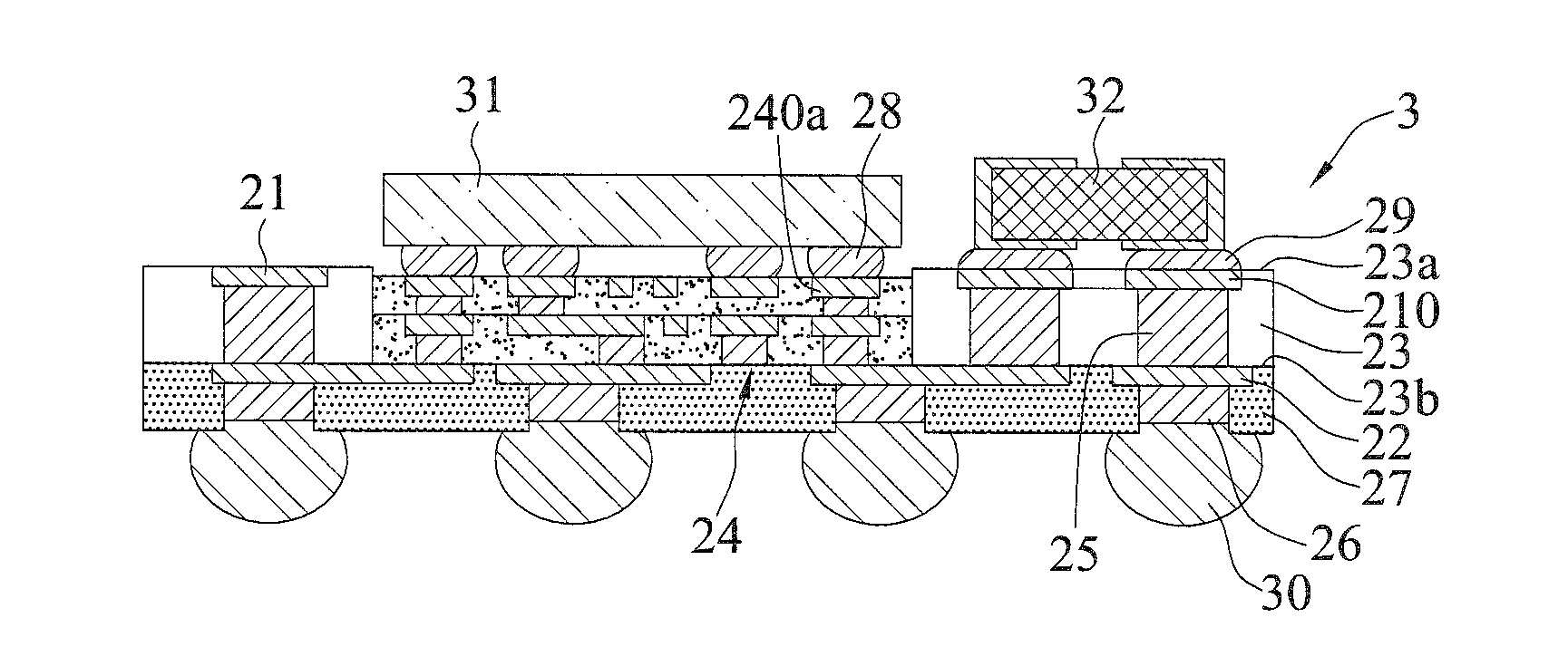
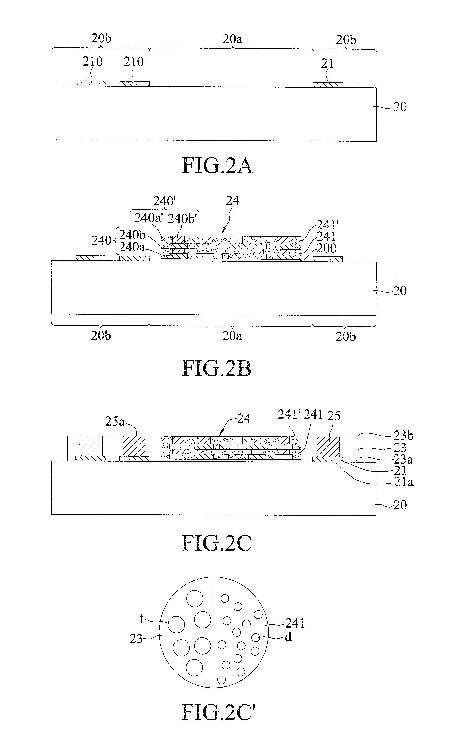
[0031]FIGS. 2A to 2F are schematic cross-sectional views showing a method for fabricating a packaging module 3 and a substrate structure 2 thereof according to the present disclosure.

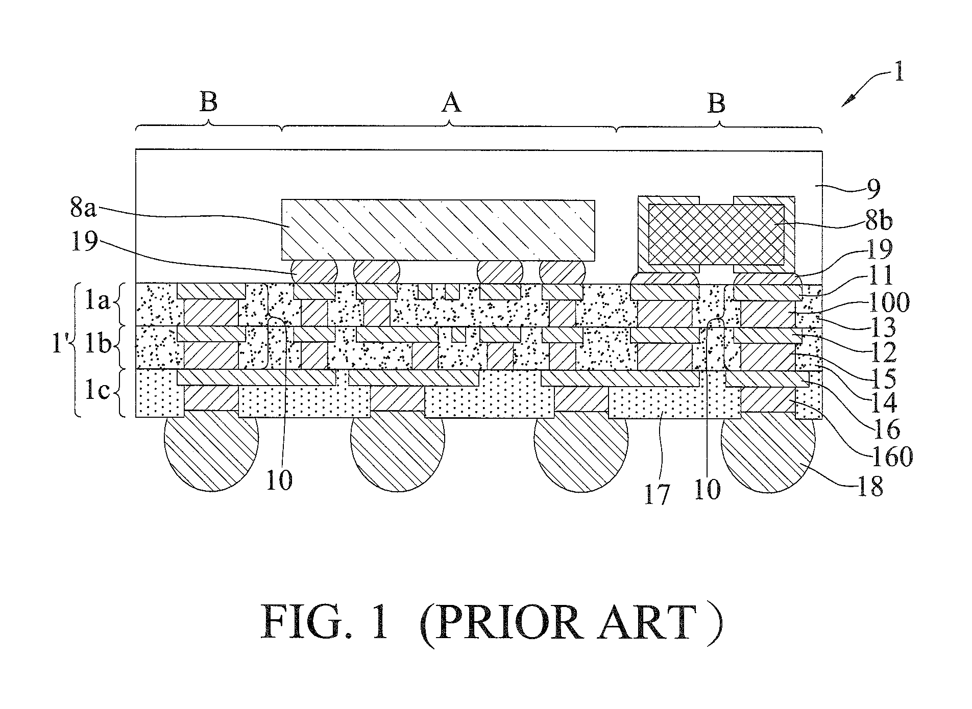
[0032]Referring to FIG. 2A, a first circuit layer 21 is formed on a carrier 20 through a patterning process.

[0033]In an embodiment, the carrier 20 is a substrate such as a copper foil substrate.

[0034]Further, a main ar...


PUM


Abstract

A substrate structure is provided, including: a circuit board having a plurality of wiring layers; a first circuit layer; a plurality of conductive posts disposed on the first circuit layer; a first insulating layer encapsulating the circuit board, the first circuit layer and the conductive posts; and a second circuit layer formed on the first insulating layer and electrically connected to the wiring layers with the second circuit layer electrically connected to the first circuit layer through the conductive posts. According to the present disclosure, fine-pitch circuits are formed in the circuit board, and thus only the circuit board needs a high-cost insulating material, thereby allowing the first insulating layer to be made of a low-cost material to reduce the fabrication cost.

Description

BACKGROUND[0001]1. Technical Field The present disclosure relates to substrate structures, and, more particularly, to a substrate structure for disposing electronic elements thereon.[0002]2. Description of Related Art[0003]Along with the rapid development of electronic industries, electronic products are developed toward the trend of miniaturization and multi-function. Accordingly, there have been developed various kinds of packaging modules.[0004]FIG. 1 is a schematic cross-sectional view of a conventional packaging module 1. The packaging module 1 has a substrate structure 1′, an active element 8a and a passive element 8b disposed on the substrate structure 1′, and an encapsulant 9 encapsulating the active element 8a and the passive element 8b. [0005]The substrate structure 1′ has a first circuit layer 11, a plurality of first conductive posts 100 disposed on the first circuit layer 11, a first insulating layer 13 encapsulating the first circuit layer 11 and the first conductive p...

Claims


Application Information

Patent Timeline
Patent Type & Authority Applications(United States)
IPC IPC(8): H01L23/498H01L21/48H01L21/56H01L23/31
CPCH01L23/49838H01L23/49822H01L23/49827H01L23/49811H01L21/565H01L21/4857H01L21/486H01L21/4853H01L23/3114H01L2224/16225H01L2924/15311H01L2924/19105H01L23/49816H01L23/49894H01L23/49833H01L23/50
Inventor HU, WEN-HUNG
Owner PHOENIX PIONEER TECH
Why Eureka
Try Eureka