Semiconductor device including drivers

a technology of semiconductor devices and drivers, applied in the direction of semiconductor devices, electrical devices, transistors, etc., can solve the problems of reducing the width of transistors capable of being realized within a predetermined region, deterioration of transistor characteristics, and difficulty in ensuring sufficient space needed to construct a layout of constituent elements and lines in highly integrated semiconductor devices, so as to maximize the driving ability of drivers and improve the arrangement structure of drivers

Active Publication Date: 2017-03-02
SK HYNIX INC
View PDF8 Cites 2 Cited by
  • Summary
  • Abstract
  • Description
  • Claims
  • Application Information

AI Technical Summary

Benefits of technology

[0010]The embodiments of the present disclosure relate to a technology for maximizing driving ability of drivers within a restricted region by improving an arrangement structure of the drivers for use in a semiconductor device.

Problems solved by technology

Generally, it is very difficult to guarantee sufficient space needed to construct a layout of constituent elements and lines in highly integrated semiconductor devices such as DRAMs.
As a result, it is difficult to adjust a Critical Dimension (CD) of the gates, and it is also impossible to properly adjust a size of a space between a contact (M0C) configured to interconnect a metal line and an active region and each gate, resulting in deterioration of transistor characteristics.
In addition, since each driver includes two gate fingers in the arrangement structure shown in FIG. 1, a transistor width capable of being realized within a predetermined region is reduced such that a driving ability of the transistor is deteriorated.
As a result, the dishing and erosion amount unavoidably increases during ISO (isolation) Chemical Mechanical Polishing (CMP), such that modification of an ISO layer occurs, resulting in deterioration of circuit throughput.

Method used


Image

  • Semiconductor device including drivers
  • Semiconductor device including drivers
  • Semiconductor device including drivers

Examples


Embodiment Construction

[0021]Reference will now be made in detail to certain embodiments, examples of which are illustrated in the accompanying drawings. Wherever possible, the same reference numbers will be used throughout the drawings to refer to the same or like parts. In the following description, a detailed description of related known configurations or functions incorporated herein will be omitted when it may make the subject matter less clear.

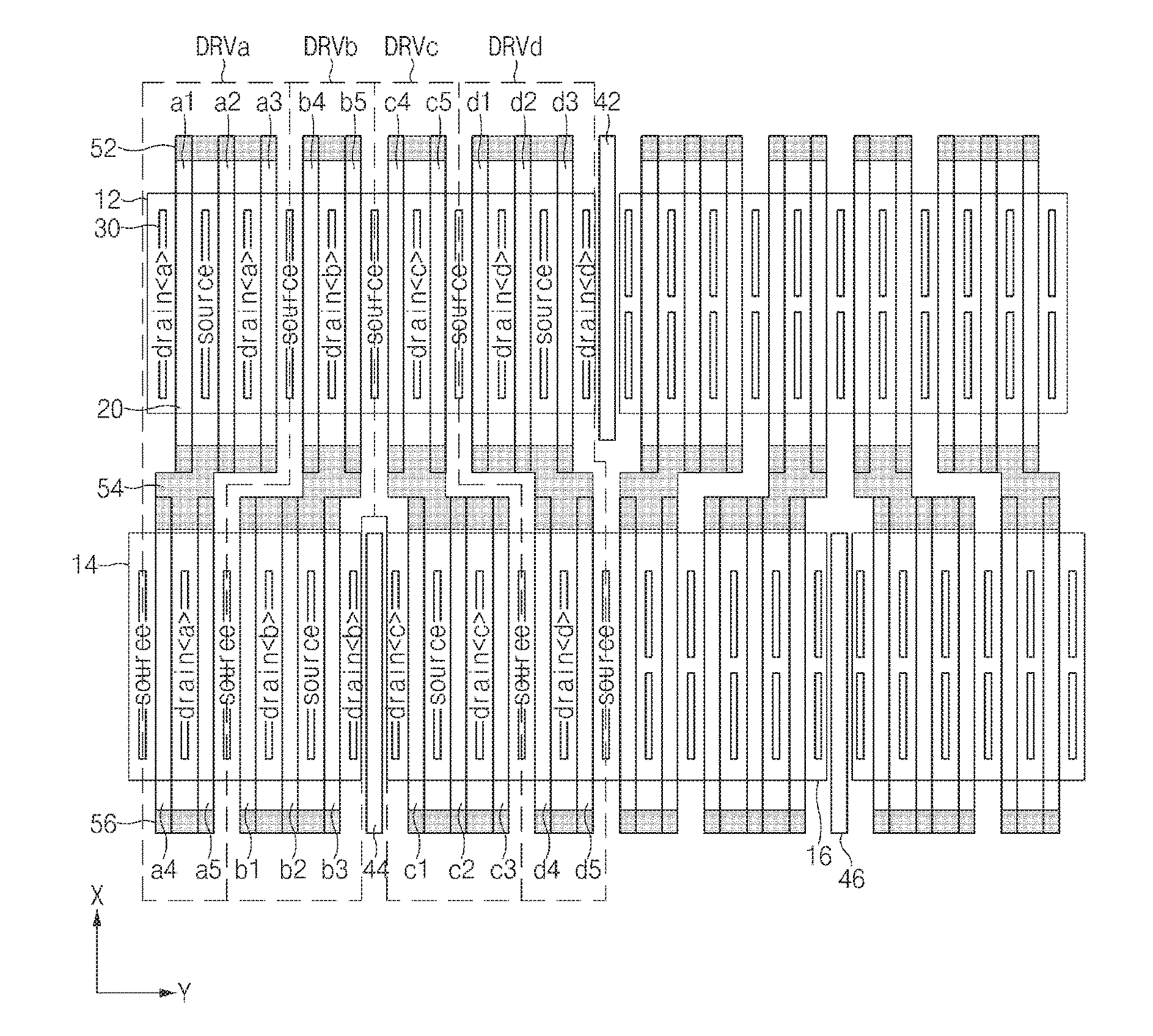
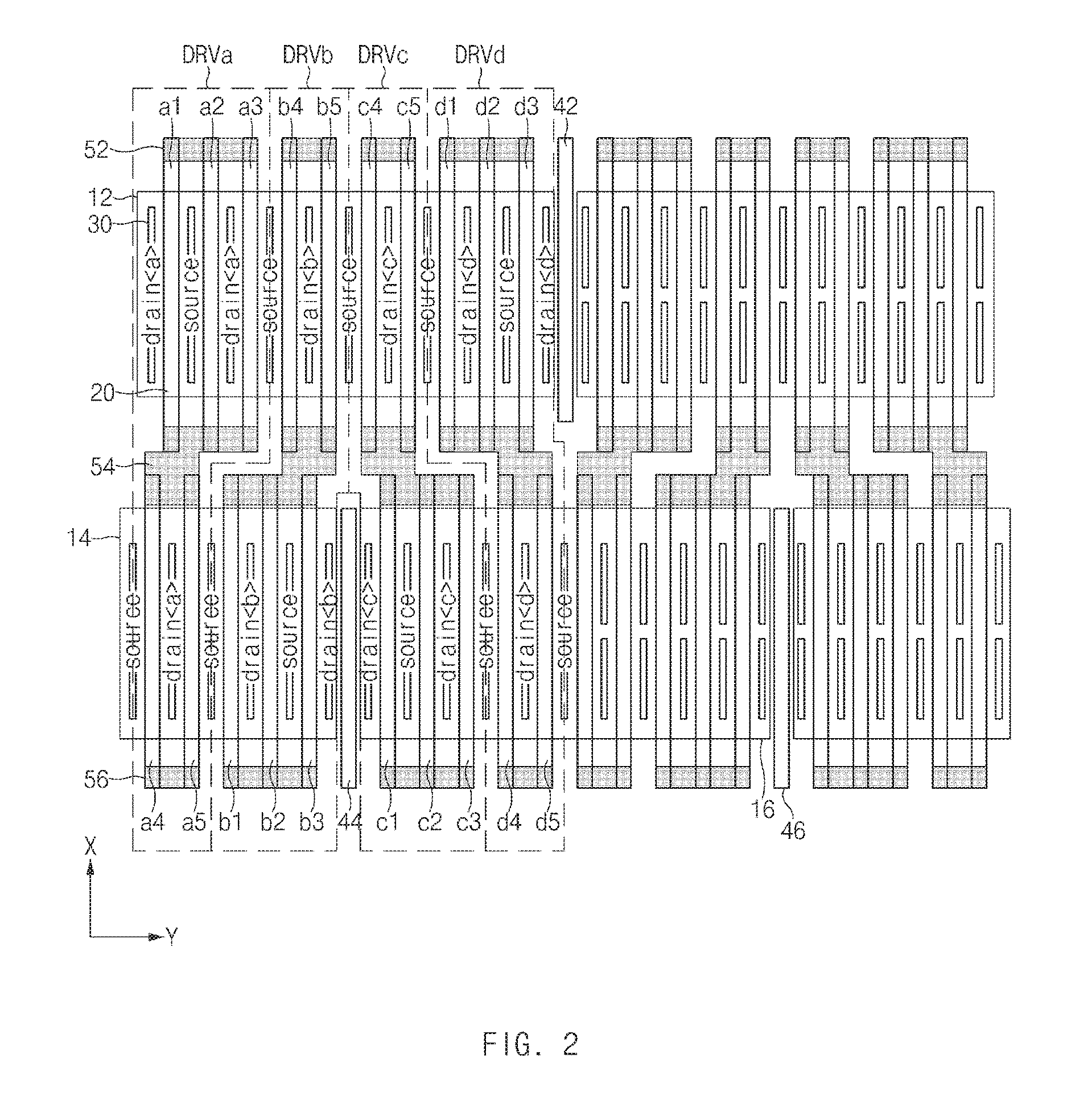
[0022]FIG. 2 is a plan view illustrating an arrangement structure of drivers according to an embodiment of the present disclosure.

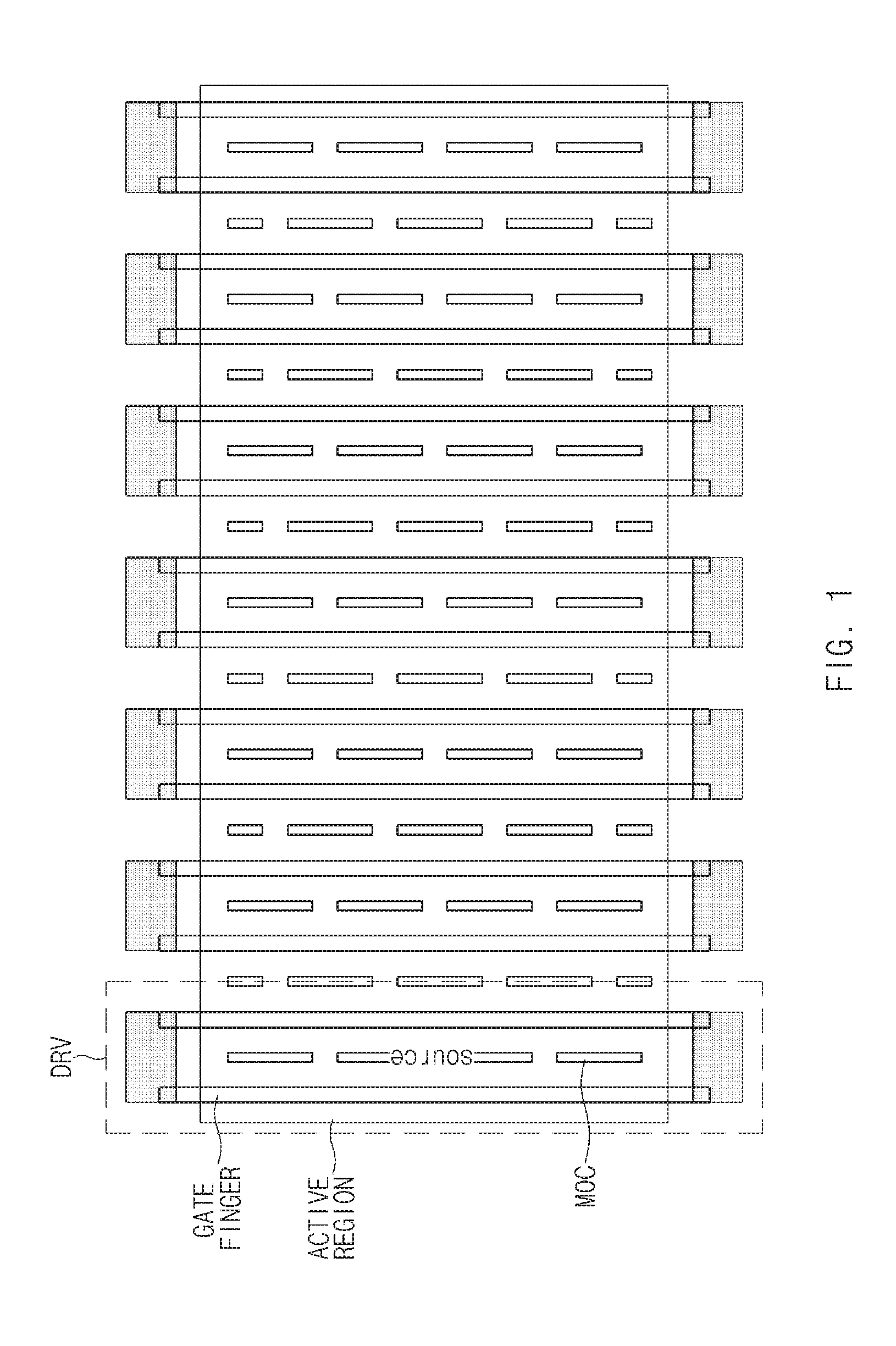
[0023]FIG. 2 illustrates an example case in which 5 finger gates 20 are formed in one driver according to an embodiment of the present disclosure. Although only some drivers (DRVa˜DRVd) are shown in FIG. 2 for convenience of description, the scope or spirit of the present disclosure is not limited thereto.

[0024]Referring to FIG. 2, a driver (DRVa) may include an odd number of gate fingers (i.e., 5 gate fingers) (a1˜a5) electrically ...


PUM


Abstract

A semiconductor device including drivers is disclosed, which can maximize driving ability of a plurality of drivers installed in a given region when the plurality of drivers is arranged in an array shape. The semiconductor device includes: a first active region; a second active region spaced apart from the first active region a predetermined distance in a first direction; a first gate finger group located in the first active region, and configured to include an odd number of gate fingers; and a second gate finger group located in the second active region, and configured to include an even number of gate fingers electrically coupled to the gate fingers of the first gate finger group.

Description

CROSS-REFERENCE TO RELATED APPLICATION[0001]The present application claims priority to Korean patent application No. 10-2015-0120034 filed on 26 Aug. 2015, the disclosure of which is hereby incorporated in its entirety by reference.BACKGROUND OF THE INVENTION[0002]Embodiments of the present disclosure relate to a semiconductor device, and more particularly to a semiconductor device configured to maximize driving ability of a plurality of drivers installed in a given region when the plurality of drivers is arranged in an array.[0003]Generally, it is very difficult to guarantee sufficient space needed to construct a layout of constituent elements and lines in highly integrated semiconductor devices such as DRAMs. Accordingly, it is very important to properly arrange constituent elements and lines within a restricted space in terms of a layout aspect.[0004]FIG. 1 is a plan view illustrating conventional arrayed drivers arranged in parallel to one another according to the related art. I...

Claims


Application Information

Patent Timeline
Patent Type & Authority Applications(United States)
IPC IPC(8): H01L27/02H01L27/108
CPCH01L27/10897H01L27/0207H01L27/088H01L28/00H10B43/27H10B12/50
Inventor LEE, SEOL HEE
Owner SK HYNIX INC
Why Eureka
Try Eureka