Eureka AIR delivers breakthrough ideas for toughest innovation challenges, trusted by R&D personnel around the world.

Semiconductor device package with seal structure

Inactive Publication Date: 2017-03-23
NXP USA INC
View PDF25 Cites 5 Cited by
  • Summary
  • Abstract
  • Description
  • Claims
  • Application Information

AI Technical Summary

Benefits of technology

The present invention provides a semiconductor device package with a seal structure that prevents air bubbles from affecting critical portions of the package. This seal structure is formed by attaching two semiconductor dies together with a seal ring pad and interconnect pads. The seal prevents air bubbles from entering the package and allows the semiconductor device to operate normally after experiencing a rapid decompression event, such as a blowout of a pressurized tire. The seal structure is formed during the manufacturing process of the semiconductor device package and includes a flag for attachment of the semiconductor die, bond leads, and a seal ring pad. The seal structure provides protection against air bubbles and ensures the reliable operation of the semiconductor device in harsh operating environments.

Problems solved by technology

However, in a rapid decompression event (RDE) such as a blowout of the pressurized tire, the bubbles can temporarily or permanently affect the operation semiconductor device.

Method used


Image

  • Semiconductor device package with seal structure
  • Semiconductor device package with seal structure
  • Semiconductor device package with seal structure

Examples


Embodiment Construction

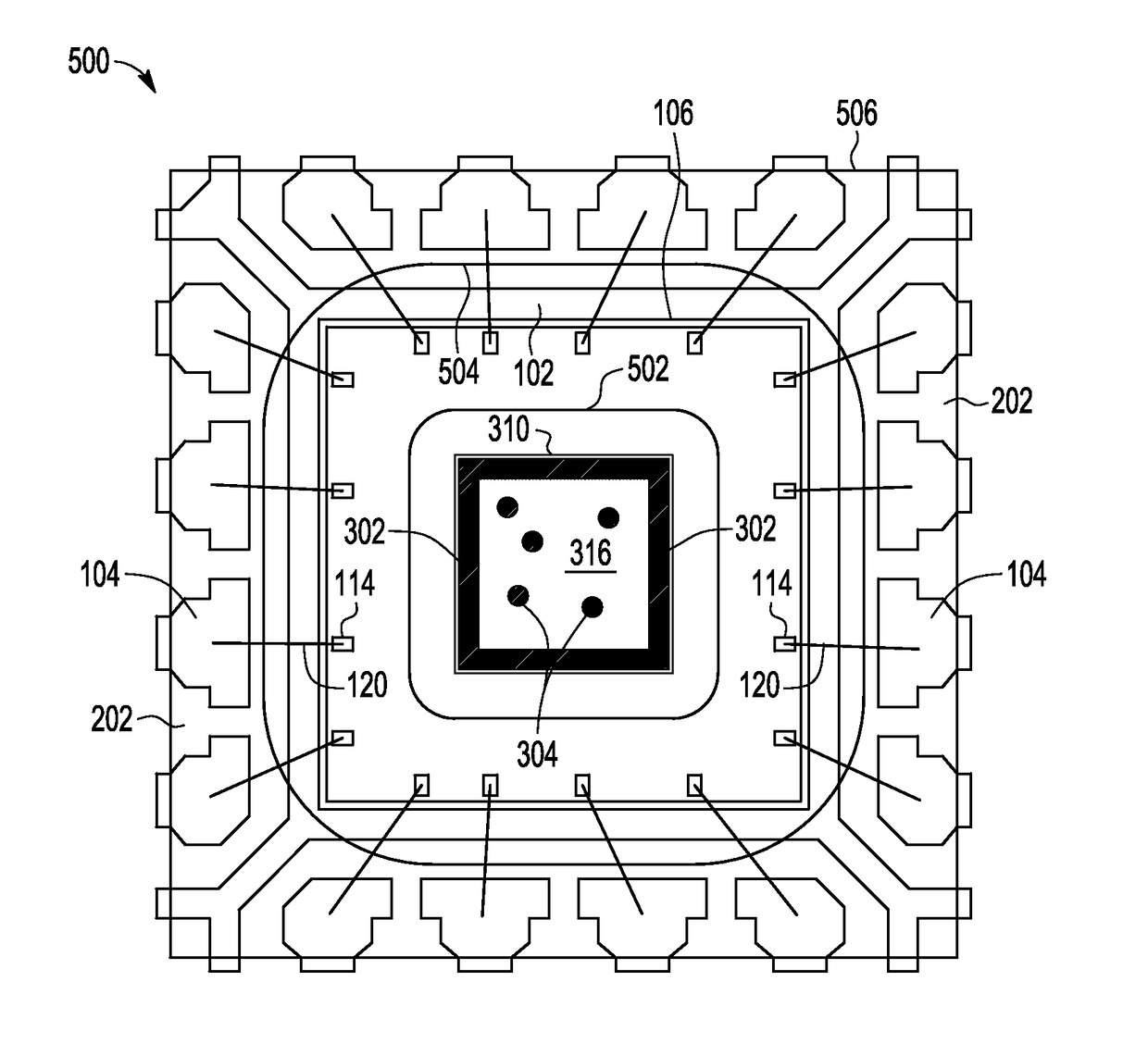
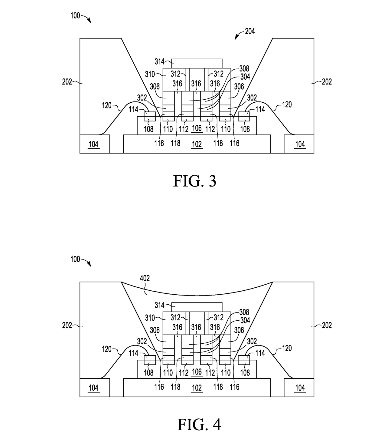
[0008]Generally, there is provided, a packaged semiconductor device that includes a first semiconductor die having a seal ring pad surrounding one or more interconnect pads and a second semiconductor die having a corresponding seal ring pad and one or more corresponding interconnect pads wherein the seal ring pad and corresponding seal ring pad are coupled to form an airtight or hermetic seal around a cavity between the first and second semiconductor die. The seal around the cavity can prevent air bubbles from permeating critical portions of the packaged semiconductor device allowing the packaged semiconductor device to operate normally after experiencing a rapid decompression event (RDE) such as a blowout of a pressurized tire.

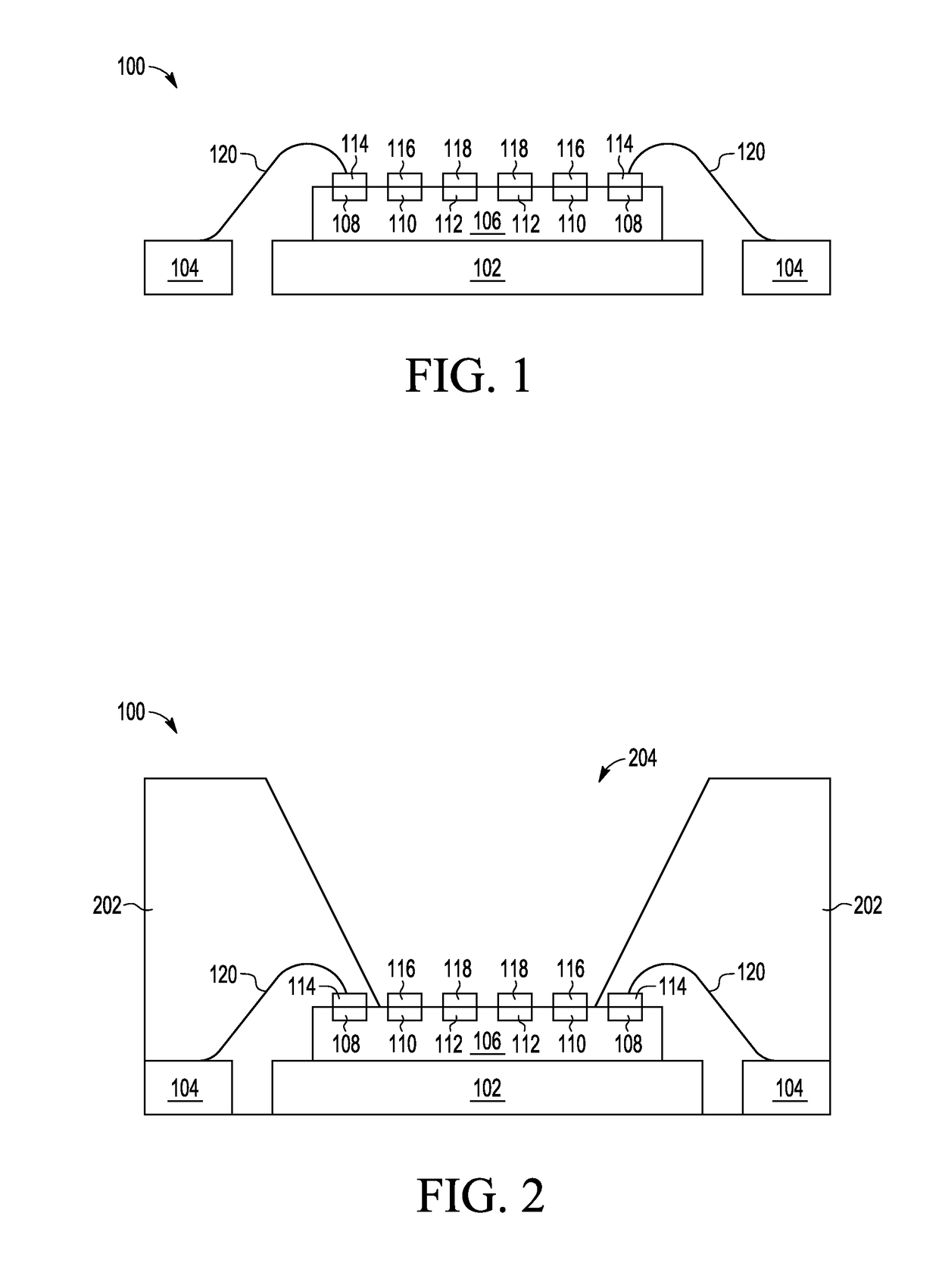
[0009]FIGS. 1-4 illustrate, in a simplified cross-sectional view, an exemplary packaged semiconductor device 100 at various stages of manufacture in accordance with an embodiment of the present disclosure.

[0010]FIG. 1 illustrates, in a simplified cross-sectio...


PUM

PropertyMeasurementUnit
Electrical conductoraaaaaaaaaa

Abstract

A packaged semiconductor device includes a first semiconductor die including interconnect pads and a seal ring pad surrounding at least some of the interconnect pads, a first portion of an plated seal ring structure formed on the seal ring pad, and a second semiconductor die including a second portion of the plated seal ring structure formed on a major surface of the second semiconductor die. The second portion of the plated seal ring structure is coupled to the first portion of the plated seal ring structure to form a seal around a cavity between the first and second semiconductor die. A plurality of interconnect pillars are on the first major surface of the second semiconductor die. The interconnect pillars are coupled to the interconnect pads on the second semiconductor die.

Description

BACKGROUND[0001]Field[0002]This disclosure relates generally to semiconductor device packaging, and more specifically, to a semiconductor device package having a seal structure.[0003]Related Art[0004]Semiconductor devices which include microelectromechanical systems (MEMS) are widely used in a variety of sensing applications. For example, a MEMS pressure sensor may be implemented on a semiconductor die to generate electrical signals indicative of the amount of pressure exerted on the semiconductor die (or a portion thereof). Often, these devices are packaged in a manner that provides protection from corrosive elements and helps ensure relatively high reliability over the lifetime of the device so that these devices may be used in harsh operating environments, such as, for example, in an automotive application. In an automotive application, a semiconductor device including a pressure sensor may be subjected to high pressure while within a pressurized tire, for example, allowing air b...

Claims


Application Information

Patent Timeline
IPC IPC(8): B81B7/00B81C1/00
CPCB81B7/0058B81C1/00301B81B2201/0264B81B2203/0127B81B2207/07B81C2203/0145B81B2207/03B81C2201/0197B81C2203/0172B81C2203/035B81C2203/0792B81B2207/094B81C1/00238B81C2203/019H01L2224/48247H01L2224/49171
Inventor SPEIGHT, THOMAS C.HOOPER, STEPHEN R.VO, NHAT D.
Owner NXP USA INC
Why Eureka
Eureka Blog
Learn More