LED display device and method for operating the same

a display device and led display technology, applied in the direction of static indicating devices, instruments, cathode-ray tube indicators, etc., can solve the problems of limiting the size of an ultrathin led display panel, limiting the size of additional memory, and reducing the design and fabrication of led display panels

Active Publication Date: 2017-03-23
SCT
View PDF5 Cites 11 Cited by
  • Summary
  • Abstract
  • Description
  • Claims
  • Application Information

AI Technical Summary

Benefits of technology

[0013]The second receivers may be serially arranged in one of the plurality of first receiver modules. The set of field information includes a first field information and a second field information. The first field information includes a first value and the second field information includes a second value. Each of the second receivers is configured to compare the first value to the second field value, and when the first number is not the same with the second number, the first number is increased by an increment of a value one (1) and the set of field information is transmitted to adjacent second receiver, and the second field information has a second number of a sequential order number of a designated second receiver.

Problems solved by technology

The design, fabrication, and operation of a large LED display panel face numerous technical challenges.
For example, the size of an LED display panel can be as large as around 7.35 m×4.1 m. With such large display panels, it becomes difficult to send a set of data to designated LED drivers across the LED display panels in a synchronous manner.
The size of the additional memory physically limit the size of an ultrathin LED display panel.
Second, the additional memory placed in the receiver card 13 for implementation of the pixel mapping function significantly increases production costs of LED display panels.
Third, the existence of an additional memory in the receiver card 13 creates an additional frame latency during pixel mapping, causing potential delays when displaying images on the LED display panel.

Method used


Image

  • LED display device and method for operating the same
  • LED display device and method for operating the same
  • LED display device and method for operating the same

Examples


Embodiment Construction

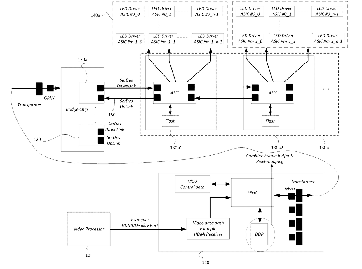
[0039]Reference will now be made in detail to embodiments, examples of which are illustrated in the accompanying drawings, wherein like reference numerals refer to the like elements throughout the several views. In this regard, the present embodiments may have different forms and should not be construed as being limited to the descriptions set forth herein. Accordingly, the embodiments are merely described below, by referring to the figures, to explain aspects of the present description. Terms used herein are for descriptive purposes only and are not intended to limit the scope of the disclosure. The terms “comprises” and / or “comprising” are used to specify the presence of stated elements, steps, operations, and / or components, but do not preclude the presence or addition of one or more other elements, steps, operations, and / or components. The terms “first,”“second,” and the like may be used to describe various elements, but do not limit the elements. Such terms are only used to dist...


PUM


Abstract

This disclosure describes an LED display device. The LED display device includes a transmitter having a memory and a pixel mapping table, a plurality of first receivers coupled to the transmitter, a plurality of second receiver modules, and a plurality of LED driver groups. A unique address is assigned to a data packet with a use of the pixel mapping table. The data packet has a set of field information and the set of field information includes the unique address. Each of the second receiver modules is coupled to at least one of the first receivers and includes a plurality of second receivers. None of the plurality of second receivers comprises a pixel mapping memory. Each of the LED driver groups is coupled to one of the plurality of second receivers and includes a plurality of LED drivers.

Description

UTILITY PATENT APPLICATION[0001]This application is a continuation-in-part application and claims benefit of U.S. non-provisional application Ser. No. 14 / 798,034, filed on Jul. 13, 2015, the disclosures of which are hereby incorporated by reference.FIELD OF THE DISCLOSURE[0002]This disclosure relates generally to an LED display device and a method for operating the same. In particular, this disclosure relates to an LED display device using a transmitter having a memory and a pixel mapping table.BACKGROUND OF THE DISCLOSURE[0003]Light emitting diode (LED) is widely used for displaying information and messages. LED is a solid-state device that converts electric energy to light. LED display panels provide a higher level of brightness and greater optical efficiency as compared to other types of display panels. Recently, LED display panels have been used to make large indoor or outdoor display panels and televisions.[0004]The design, fabrication, and operation of a large LED display pane...

Claims


Application Information

Patent Timeline
Patent Type & Authority Applications(United States)
IPC IPC(8): G09G5/395G09G5/393
CPCG09G5/395G09G5/393G09G2370/04G09G2370/02G09G2370/14G09G3/32G09G3/3208G09G5/006G09G2300/026G09G2352/00G09G2370/042G09G2370/10
Inventor LI, ERICCHEN, JUINN-YANCHIOU, SHEAN-YIHTANG, SHANG-KUAN
Owner SCT
Why Eureka
Try Eureka