Method of making a microelectronic device
- Summary
- Abstract
- Description
- Claims
- Application Information
AI Technical Summary
Benefits of technology
Problems solved by technology
Method used
Image

Examples
Embodiment Construction
[0032]Before beginning a detailed review of the embodiments of the invention, hereinafter are mentioned the optional characteristics that may be used according to any combination or alternatively:
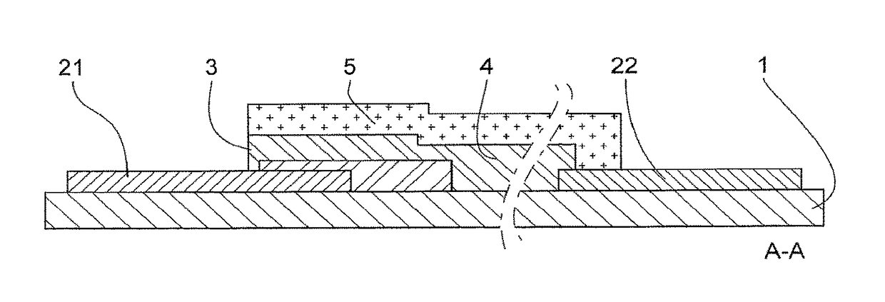
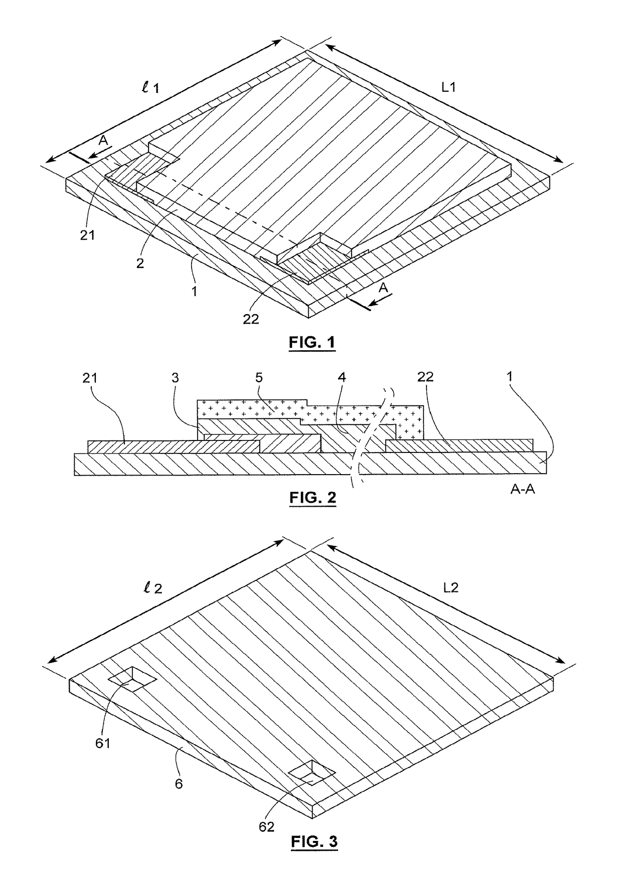
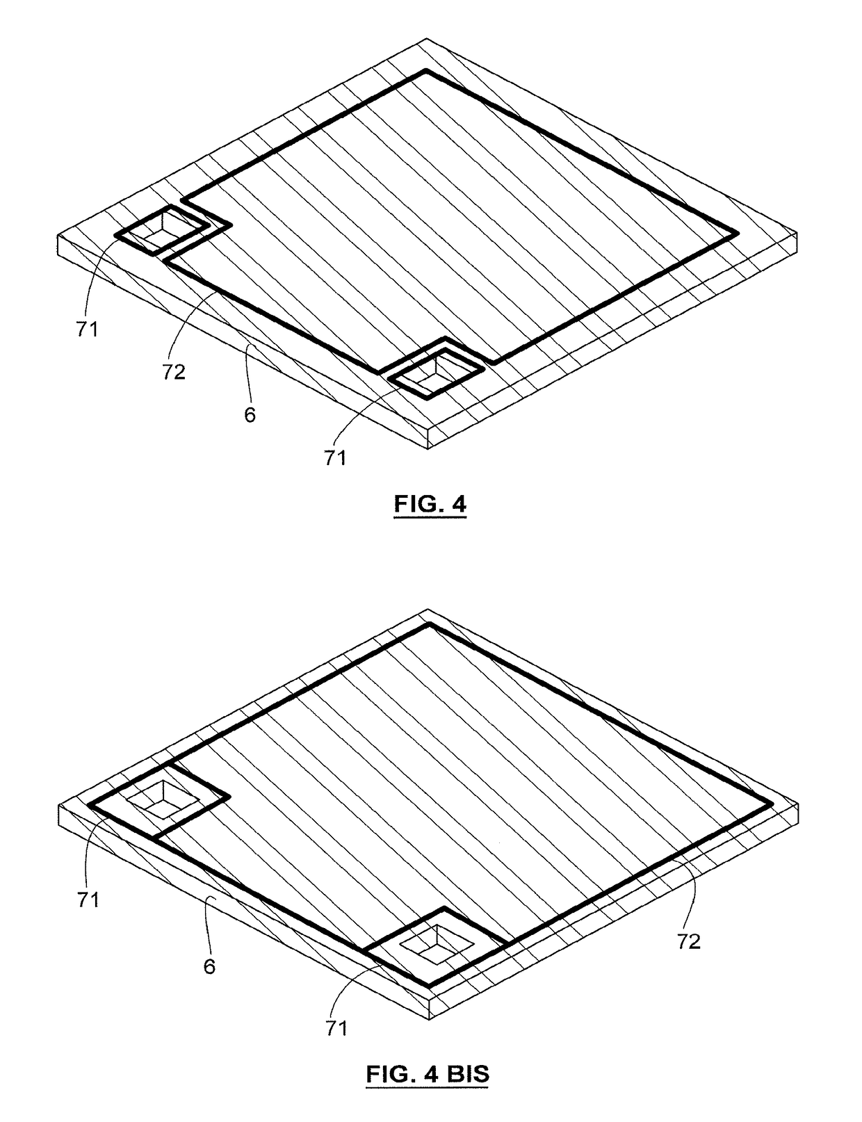
[0033]prior to the step of filling with an electrically conductive material, it is carried out in the support (1) the at least one passage (63, 64) according to a dimension in thickness of said support in such a way that the at least one passage (63, 64) passes through the at least one electrical connector (21, 22);
[0034]the step of filling is configured in such a way that the conductive material passes through the support (1) through the at least one passage (63, 64) in such a way as to be exposed on a second face of the support (1), opposite the first face.
[0035]the connector (21, 22) is positioned at the periphery of the electronic component (2).
[0036]the step of setting in place of the cover (6) is configured to preserve at least one second access to at least one second electrical conne...
PUM
 Abstract
Description
Claims
Application Information
 - R&D
- Intellectual Property
- Life Sciences
- Materials
- Tech Scout
- Unparalleled Data Quality
- Higher Quality Content
- 60% Fewer Hallucinations
Browse by: Latest US Patents, China's latest patents, Technical Efficacy Thesaurus, Application Domain, Technology Topic, Popular Technical Reports.
© 2025 PatSnap. All rights reserved.Legal|Privacy policy|Modern Slavery Act Transparency Statement|Sitemap|About US| Contact US: help@patsnap.com