Thin Film Transistor, Array Substrate and Method of Forming the Same

a thin film transistor and array substrate technology, applied in the field of display technology, to achieve the effect of preventing photoresist from shedding, ensuring evenness and smoothness of the surface, and reducing the production power of the second copper layer

Active Publication Date: 2017-05-04
TCL CHINA STAR OPTOELECTRONICS TECH CO LTD
View PDF0 Cites 1 Cited by
  • Summary
  • Abstract
  • Description
  • Claims
  • Application Information

AI Technical Summary

Benefits of technology

[0017]In the present invention, at least one of TFT's gate, source and drain adopts a structure of a first buffer layer, a first copper layer, a second copper layer and a second buffer layer. The production power of the first copper layer is higher than that of the second copper layer. The second buffer layer protects the second copper layer, preventing the problem of photoresist shedding resulted from direct etching of the copper layer. In addition, because the production power of the second copper layer is lower, it ensures evenness and smoothness of the surface of the second copper layer, and further ensures that the covering of the second buffer layer of the second copper layer is even and smooth. It prevents photoresist from shedding. Moreover, the high production power of the first copper layer also ensures the production efficiency of TFTs.

Problems solved by technology

In the process of etching, the shedding of photoresist is common, resulting in over-etching.

Method used


Image

  • Thin Film Transistor, Array Substrate and Method of Forming the Same
  • Thin Film Transistor, Array Substrate and Method of Forming the Same
  • Thin Film Transistor, Array Substrate and Method of Forming the Same

Examples


Embodiment Construction

[0023]For the purpose of description rather than limitation, the following provides such specific details as a specific system structure, interface, and technology for a thorough understanding of the application. However, it is understandable by persons skilled in the art that the application can also be implemented in other embodiments not providing such specific details. In other cases, details of a well-known apparatus, circuit and method are omitted to avoid hindering the description of the application by unnecessary details.

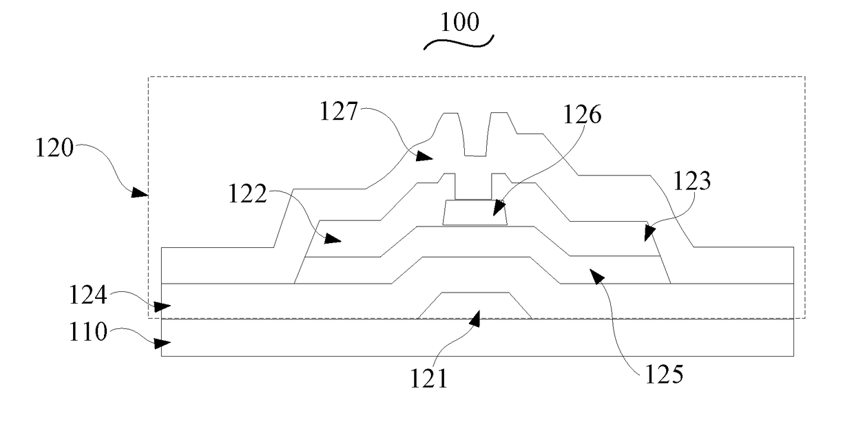
[0024]Please refer to FIG. 1. FIG. 1 is a structure diagram of an embodiment of the array substrate of the present invention. In the present embodiment, an array substrate 100 comprises a substrate 110 and a plurality of TFTs 120 (FIG. 1 only shows one TFT 120 on the substrate 110 as an example). The substrate 110 can be a transparent substrate made of glass or other insulating materials. The TFT 120 comprises a gate 121, a source 122 and a drain 123 install...


PUM

PropertyMeasurementUnit
thicknessaaaaaaaaaa
resistance-capacitanceaaaaaaaaaa
impedanceaaaaaaaaaa

Abstract

The present disclosure proposes a TFT. The source and the drain of the TFT are disposed on the same side as the gate. The gate includes a first buffer layer, a first copper layer, a second copper layer and a second buffer layer that are stacked from bottom to top, and the second buffer layer is disposed on the side that is close to the source and drain. The source and drain include a first buffer layer, a first copper layer, a second copper layer and a second buffer layer that are stacked, and the first buffer layer is disposed on the side that is close to the gate. The first copper layer is deposited by a first power, the second copper layer is deposited by a second power lower than the first power. Through the above method, it is prevents photoresist from shedding when etching.

Description

BACKGROUND OF THE INVENTION[0001]1. Field of the Invention[0002]The present invention relates to the field of display technology, and more specifically, to a thin-film transistor (TFT), an array substrate and a method of forming the same.[0003]2. Description of the Prior Art[0004]In the field of liquid crystal display (LCD), an array substrate installed with TFTs serves as a switch of the LCD panel, whose structure and technology is gravely important to its display effect. To respond to a current need of large-size display device and reduce problems such as resistance-capacitance (RC) delay, a TFT with its gate, source and drain made of low-cost, low-impedance copper is apparently the best choice.[0005]In a conventional production procedure of TFTs, the gate, source and drain of TFTs usually adopt a structure composed of stacked molybdenum layers and copper layers, or titanium layers and copper layers. The molybdenum layer and titanium layer serve as buffer layers. When making TFTs,...

Claims


Application Information

Patent Timeline
Patent Type & Authority Applications(United States)
IPC IPC(8): H01L27/12H01L29/45H01L29/66H01L29/423H01L21/443H01L29/786H01L29/49H01L29/417
CPCH01L27/1225H01L29/4908H01L29/45H01L29/41733H01L29/66969H01L21/443H01L27/1259H01L29/7869H01L29/42372H01L27/1214H01L29/42384H01L29/786
Inventor ZHOU, ZHICHAOWU, YUE
Owner TCL CHINA STAR OPTOELECTRONICS TECH CO LTD
Why Eureka
Try Eureka