

Method for manufacturing electronic device, and electronic device
a technology of electronic devices and manufacturing methods, applied in the direction of semiconductor/solid-state device details, printed circuit non-printed electric components association, other domestic articles, etc., can solve the problems of further restricting the penetration of the substrate through the hole by the constituent material, and restricting the size of the substrate. , to achieve the effect of restricting the siz
- Summary
- Abstract
- Description
- Claims
- Application Information
AI Technical Summary
Benefits of technology
Problems solved by technology
Method used
Image

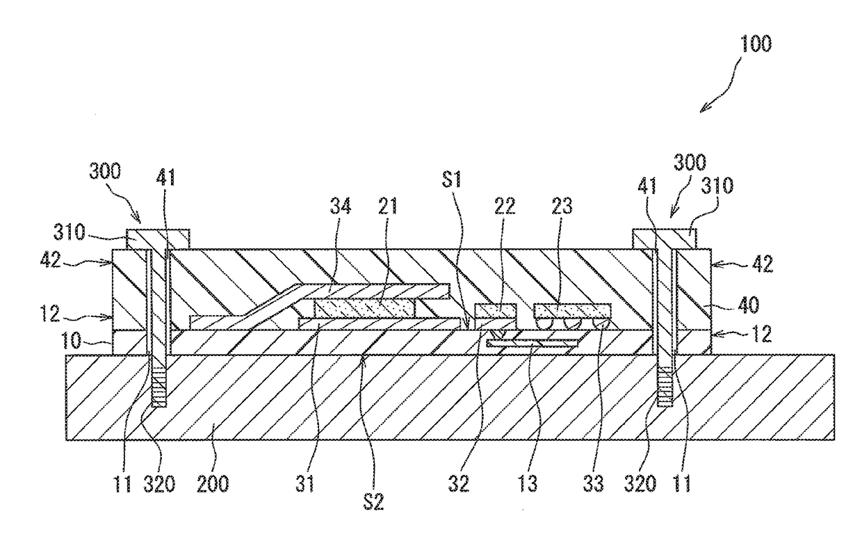
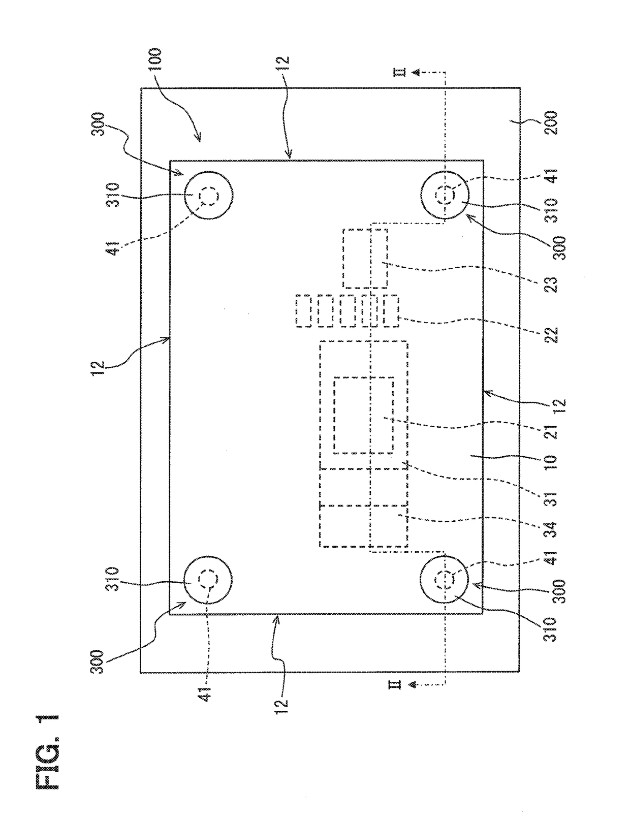
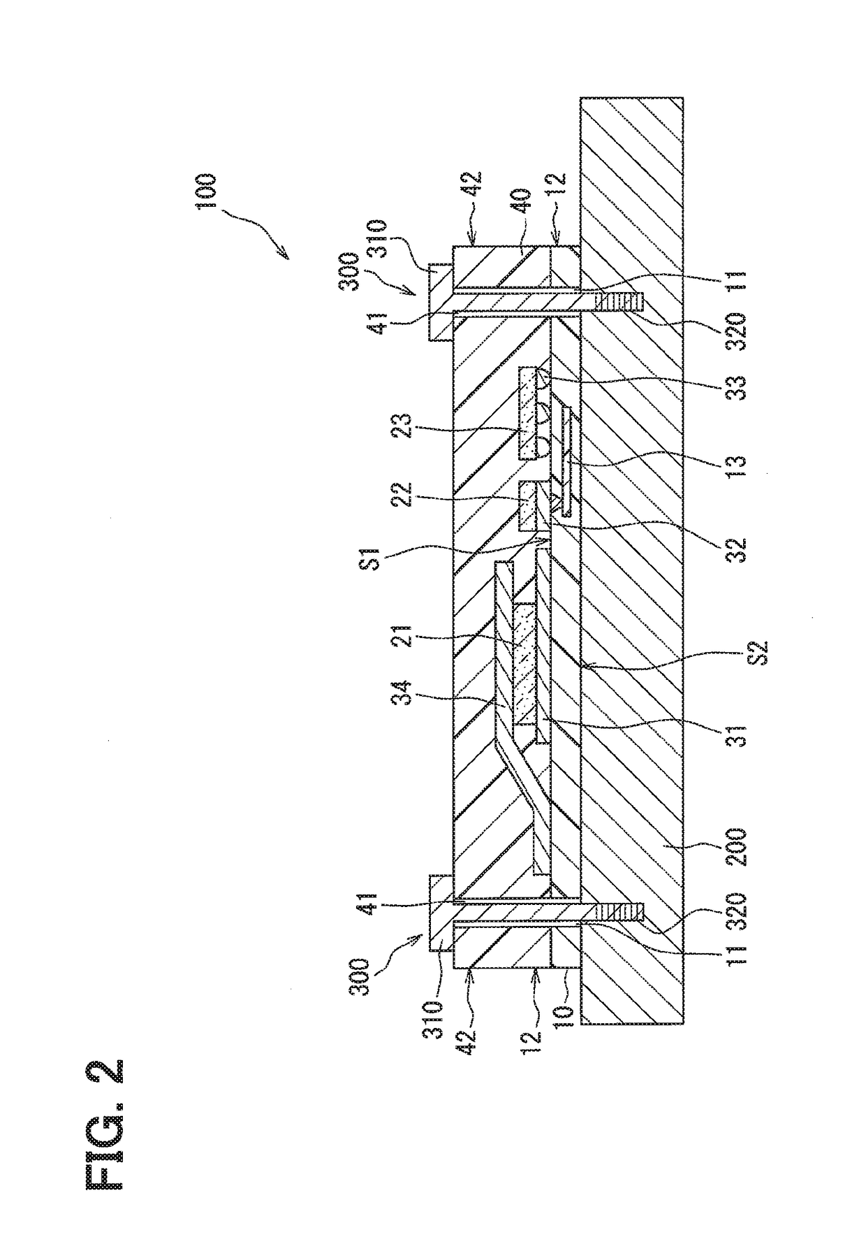
Examples
first modification example
[0108]An electronic device according to the first modification example has a circuit board 10a. In the circuit board 10a, conductive portions 14 are disposed on inner wall surfaces of through holes in the resin base material as illustrated in FIG. 17. In other words, the substrate through hole 11 is disposed between the conductive portions 14 in the circuit board 10a.
[0109]A metal such as copper constitutes this conductive portion 14 and the conductive portion 14 is equivalent to a conductive member. The conductive portion 14 is disposed in an annular shape over an entire circumference of the through hole in the resin base material and is also disposed on a part of the surface S1 and a part of the reverse surface S2. In other words, a region of the circuit board 10a that is surrounded by portions of the conductive portions 14 placed in the through holes in the resin base material is the substrate through hole 11. The inner wall surface means a surface that is exposed to the through...
second modification example
[0116]An electronic device according to the second modification example has a circuit board 10b. In the circuit board 10b, a conductive portion 141 is disposed on the inner wall surface of the through hole in the resin base material as illustrated in FIG. 21. This conductive portion 141 differs in shape from the conductive portion 14. The circuit board 10b is provided with the conductive inclined portion 14a and the resin inclined portion 11a as in the case of the circuit board 10a.
[0117]The conductive portion 141 is provided with a conductive flat portion 14b that is parallel to a thickness direction of the circuit board 10b. In the circuit board 10b, the conductive flat portion 14b is provided further on the reverse surface S2 side than the conductive inclined portion 14a. The conductive flat portion 14b is provided to be continuous with respect to the conductive inclined portion 14a via a portion along the thickness direction. A resin flat portion 11b, which is deformed when the...
third modification example
[0120]As illustrated in FIG. 22, an electronic device according to the third modification example has a circuit board 10c in which a dam portion 15 is disposed on a surface of the conductive portion 14. The dam portion 15 is provided in an annular shape on the conductive portion 14 and is sealed by the mold resin 40. The dam portion 15 is provided on the conductive portion 14 before the mold resin 40 is provided. By the dam portion 15 being disposed in advance in the circuit board 10c, the electronic device according to the third modification example can be manufactured by a method similar to the method for manufacturing the electronic device according to the first modification example.
[0121]The third modification example is capable of achieving effects similar to those achieved by the embodiment described above. In the electronic device according to the third modification example, a progress of peeling of an interface between the conductive portion 14 and the mold resin 40 can be r...
PUM
| Property | Measurement | Unit |
|---|---|---|
| thickness | aaaaa | aaaaa |
| area | aaaaa | aaaaa |
| diameter | aaaaa | aaaaa |
Abstract
Description
Claims
Application Information