Array substrate, touch display device and driving method thereof

a touch display device and substrate technology, applied in the direction of digital storage, instruments, computing, etc., can solve the problem of not meeting the user's requirement for the narrow frame of the display panel, and achieve the effect of reducing the area occupied by the non-display region and increasing the sensitiveness of touch detection

Active Publication Date: 2017-05-25
XIAMEN TIANMA MICRO ELECTRONICS +1
View PDF5 Cites 19 Cited by
  • Summary
  • Abstract
  • Description
  • Claims
  • Application Information

AI Technical Summary

Benefits of technology

[0014]According to the technical solution of the present disclosure, the shift registers disposed at at least one side of the peripheral region are divided into N groups of shift registers. The touch driving circuit comprises N groups of touch selection outputting units corresponding to the N groups of shift registers. The number of the stages of touch selection output units in each of the N groups of touch selection output units is less than the number of the stages of shift registers in each of the N groups of shift registers. Each stage of touch selection output unit includes a strobe signal input terminal, and the strobe signal input terminal of each stage of touch selection output units in each group of touch selection output units is electrically connected with secondary trigger signal output terminals of different stages of shift registers in corresponding one of the N groups of shift registers. When the touch display device is driven, a scan phase of each display frame is divided into N time periods, and sequentially driving each group of shift registers and causing each stage of shift register in each group of shift registers to output a display scan signal and a secondary trigger signal, outputting a touch driving signal according to the secondary trigger signal received by the strobe signal input terminal by each stage of touch selection output unit in each group of touch selection output units. The shift register in the gate electrode driving circuit provides a display scan signal for display and provides a touch driving signal for touch. As a result, as compared with the related art, it is not necessary to separately arrange a touch scan circuit, and hence the area occupied by the non-display region can be decreased, meeting the requirement for narrow-frame of the display panel by the user. In addition, N touch scans are performed in the scan phase of each display frame, so that it is realized that the touch scan effect of the N frequency doublings, thereby making the touch detecting more sensitive.

Problems solved by technology

As a result, it cannot meet the requirement for the narrow-frame of the display panel by the user.

Method used


Image

  • Array substrate, touch display device and driving method thereof
  • Array substrate, touch display device and driving method thereof
  • Array substrate, touch display device and driving method thereof

Examples


Embodiment Construction

[0026]The present disclosure will be described clearly and utterly in combination with the accompanying drawings and the embodiments in the present disclosure. It should be understood that the embodiments described herein are only part of embodiments. Based on the embodiments described in the present disclosure, other embodiments, obtained without any creative work, belong to the scope sought to be protected in the present disclosure.

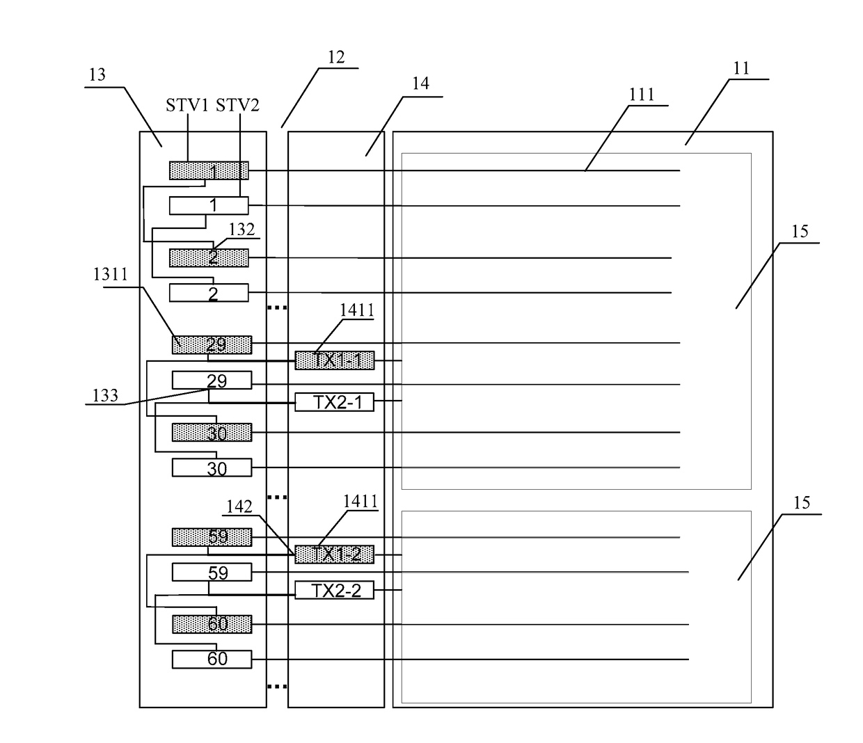
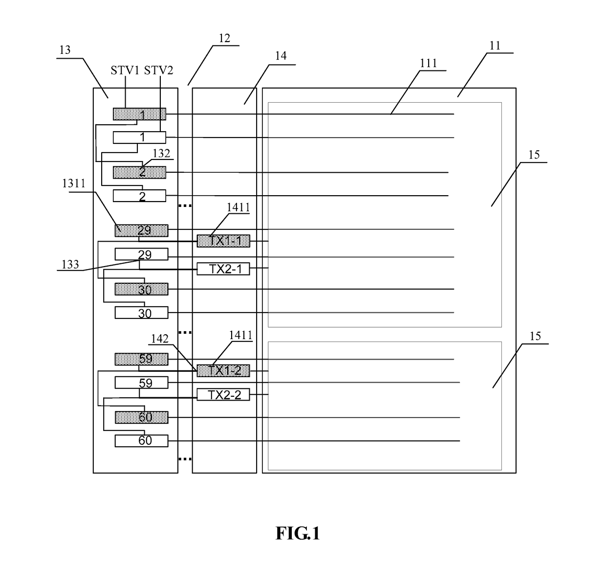
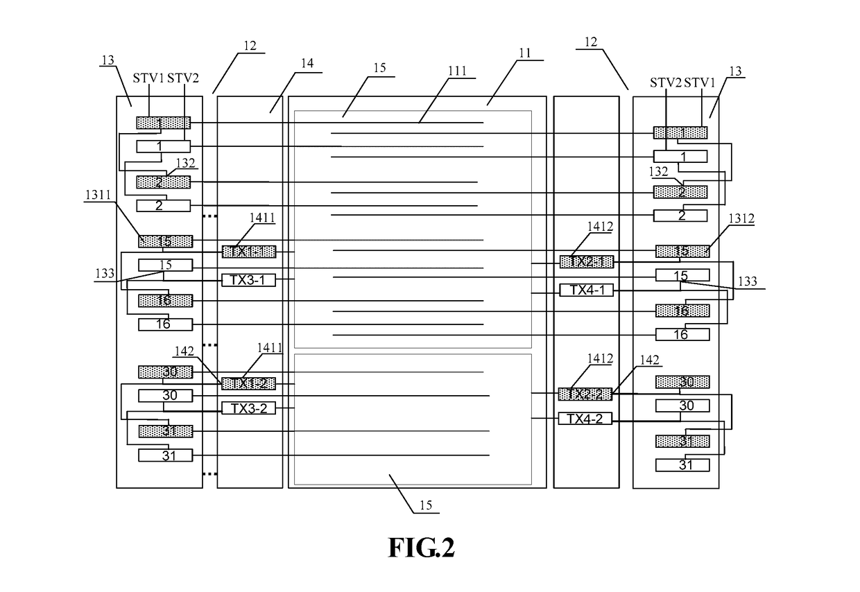
[0027]FIG. 1 is a schematic view showing the structure of an array substrate according to an embodiment of the present disclosure. As shown in FIG. 1, the array substrate includes a display region 11 and a peripheral region 12 around the display region 11. The display region 11 includes a plurality of scan lines 111 and the peripheral region 12 includes a gate electrode driving circuit 13 and a touch driving circuit 14. The gate electrode driving circuit 13 includes a plurality of stages of shift registers 131, each of the plurality of stages of shift r...


PUM

PropertyMeasurementUnit
timeaaaaaaaaaa
thicknessaaaaaaaaaa
areaaaaaaaaaaa

Abstract

The disclosure provides an array substrate, a touch display device and a driving method thereof. The array substrate includes a display region and a peripheral region. The display region includes a plurality of scan lines and the peripheral region comprises a gate electrode driving circuit and a touch driving circuit, the gate electrode driving circuit includes a plurality of stages of shift registers. Each of the plurality of stages of shift registers corresponds to and is electrically connected to one of the plurality of scan lines. The plurality of stages of shift registers are disposed at one side or two sides of the peripheral region. The shift registers disposed at at least one side of the peripheral region are divided into N groups of shift registers. The touch driving circuit includes N groups of touch selection outputting units corresponding to the N groups of shift registers.

Description

CROSS-REFERENCES TO RELATED APPLICATIONS[0001]This application claims priority to a Chinese patent application No. 201510824125.0 filed on Nov. 24, 2015 and entitled “Array Substrate, Touch Display Device and Driving Method thereof”, the disclosure of which is incorporated herein by reference in its entirety.TECHNICAL FIELD[0002]The present disclosure relates to the field of liquid crystal display technologies, in particular to an array substrate, a touch display device and a driving method thereof.TECHNICAL BACKGROUND[0003]In the field of display technologies, display function and touch display provided in more and more products are integrated into a same display panel, thereby effectively reducing a thickness of a display panel. Among them, an in-cell touch display panel has a better performance in reducing the thickness.[0004]The in-cell touch display panel is configured to integrate a plurality of touch driving electrodes onto an array substrate and perform a driving operation t...

Claims


Application Information

Patent Timeline
Patent Type & Authority Applications(United States)
IPC IPC(8): G06F3/041G02F1/1335G11C19/28G02F1/1333
CPCG06F3/0416G06F3/0412G11C19/28G02F1/133514G02F1/13338G11C19/287G09G3/20G09G3/3677G09G2310/0286G09G2354/00G06F3/04166G06F3/0446G06F3/04164G06F3/0445
Inventor SUN, YING
Owner XIAMEN TIANMA MICRO ELECTRONICS
Why Eureka
Try Eureka