

Method of atomic layer etching using functional group-containing fluorocarbon
a fluorocarbon and functional group technology, applied in the field of atomic layer etching, can solve the problems of inability to achieve good inability to achieve in-plane uniformity, and failure to meet the above requirements of conventional etchant gases, etc., to achieve the effect of improving in-plane uniformity of etching
Active Publication Date: 2017-06-29
ASM IP HLDG BV
View PDF4 Cites 206 Cited by
- Summary
- Abstract
- Description
- Claims
- Application Information
AI Technical Summary
Benefits of technology
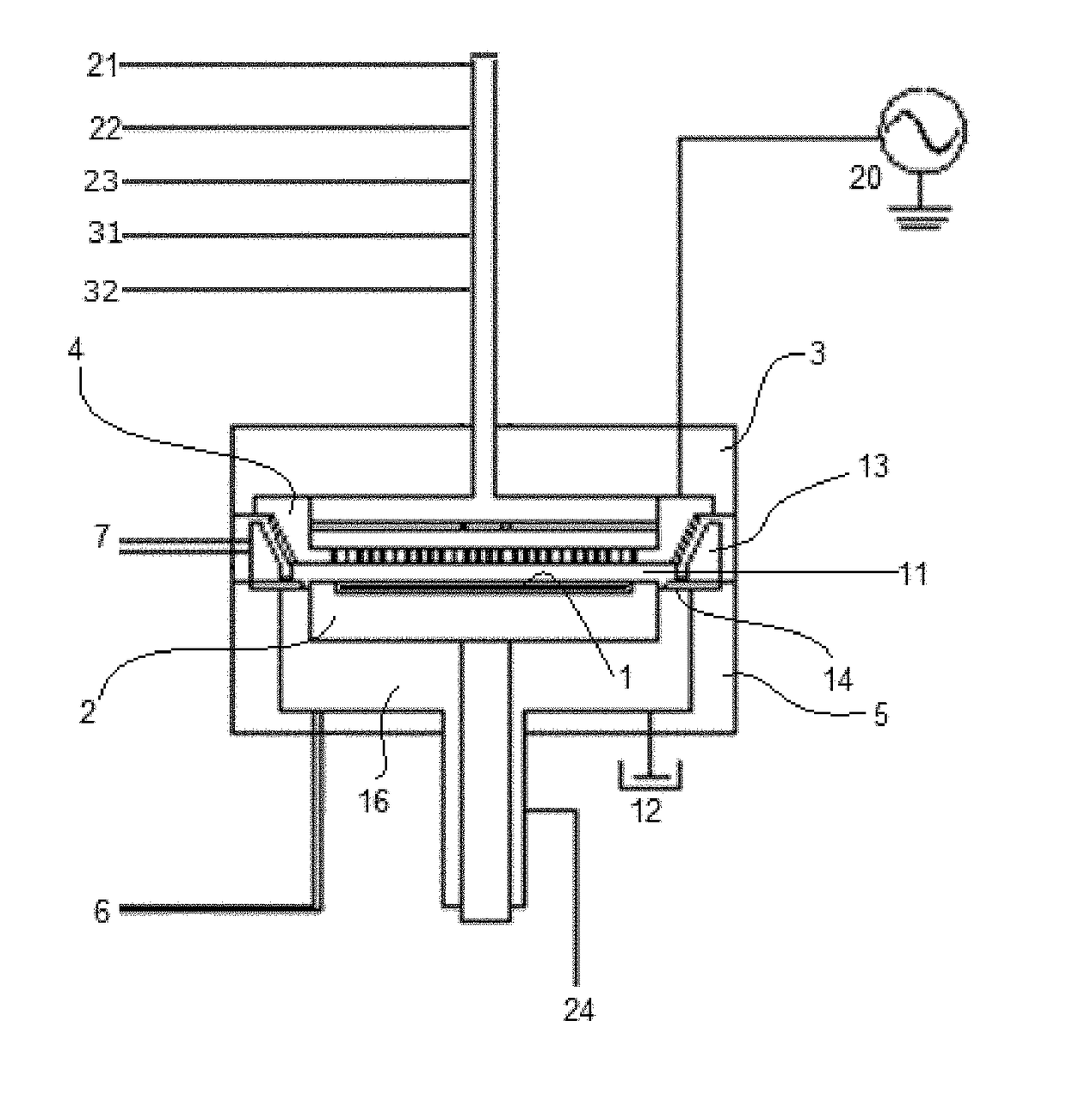
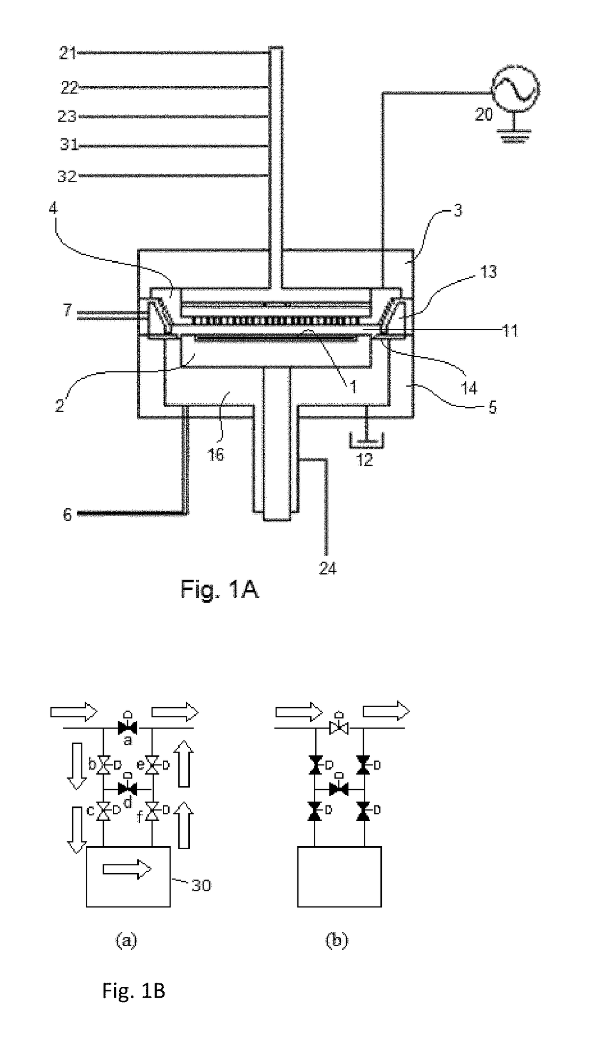
[0008]In some embodiments, by adsorbing an etchant gas on a surface of a metal or silicon oxide or nitride substrate (e.g., SiO2 substrate) in a self-limiting manner, ALE cycles (e.g., plasma-enhanced ALE or PEALE, thermal ALE, radical ALE) are performed to etch the surface, thereby improving in-plane uniformity of etching. In some embodiments, such an etchant is typically liquid at room temperature, the etchant is introduced into a reaction chamber using a flow-path switching (FPS) method wherein a carrier gas
Problems solved by technology
However, when etching a silicon oxide or silicon nitride film by ALE using a fluorocarbon such as C4F8 as an etchant gas, good in-plane uniformit
Method used
View moreImage
Smart ImageViewing Examples

Examples
 PUM
 Abstract
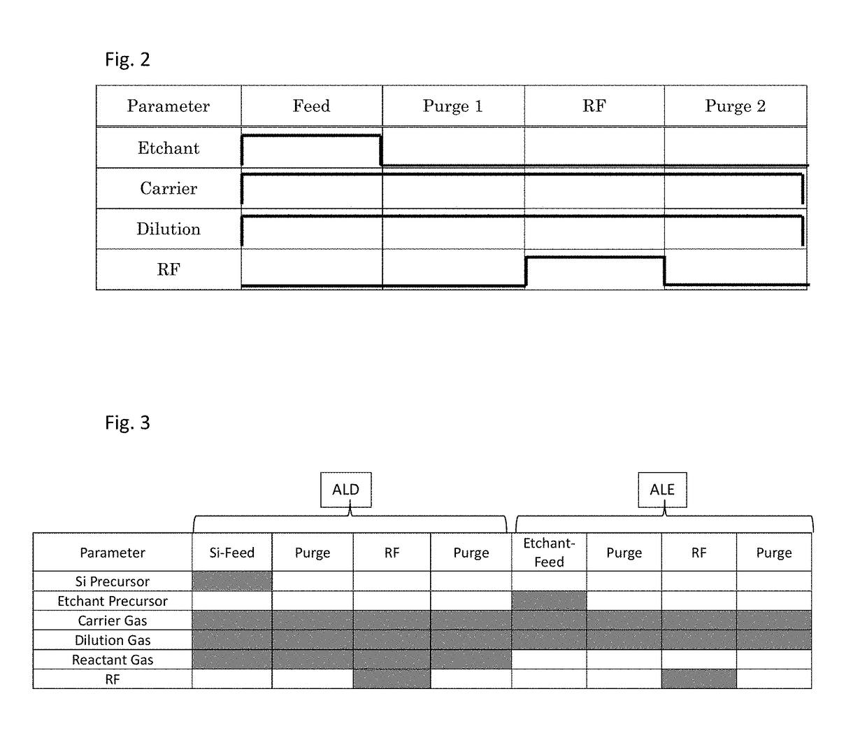
A method of atomic layer etching (ALE) uses a cycle including: continuously providing a noble gas; providing a pulse of an etchant gas to the reaction space to chemisorb the etchant gas in an unexcited state in a self-limiting manner on a surface of a substrate in the reaction space; and providing a pulse of a reactive species of a noble gas in the reaction space to contact the etchant gas-chemisorbed surface of the substrate with the reactive species so that the layer on the substrate is etched. The etchant gas is a fluorocarbon gas containing a functional group with a polarity.
Description
BACKGROUND OF THE INVENTION[0001]Field of the Invention[0002]The present invention generally relates to a method of atomic layer etching (ALE), particularly to a method of ALE using a functional group-containing fluorocarbon etchant.[0003]Description of the Related Art[0004]Atomic layer etching (ALE) is cyclic, atomic layer-level etching using an etchant gas adsorbed on a target film and reacted with excited reaction species, as disclosed in Japanese Patent Laid-open Publication No. 2013-235912 and No. 2014-522104. As compared with conventional etching technology, ALE can perform precise, atomic layer-level continuous etching on a sub-nanometer order to form fine, narrow convex-concave patterns and may be suitable for e.g., double-patterning processes. As an etchant gas, Cl2, HCl, CHF3, CH2F2, CH3F, H2, BCL3, SiCl4, Br2, HBr, NF3, CF4, C2F6, C4F8, SF6, O2, SO2, COS, etc. are known. However, it is revealed that in-plane uniformity of etching of a film on a substrate by ALE is not sat...
Claims
Login to View More Application Information
Patent Timeline
 IPC IPC(8): H01L21/311H01L21/02
CPCH01L21/31116H01L21/0228H01L21/32137H01L21/32136H01L21/67069H01J37/32146H01L21/3065H01L21/31122H01J37/32174H01J37/3244H05H1/46
InventorZAITSU, MASARU
OwnerASM IP HLDG BV