Table for plasma processing apparatus and plasma processing apparatus

a plasma processing apparatus and plasma technology, applied in the direction of chemical vapor deposition coating, electric discharge tubes, coatings, etc., can solve the problems of difficult to cover such holes with alumite, difficult to provide a result of the process excellent in the in-plane uniformity, uneven electron density of generated plasma, etc., to avoid or suppress the damage of the electrostatic chuck, the effect of suppressing the stress on the electrostatic chuck

Inactive Publication Date: 2009-04-23
TOKYO ELECTRON LTD
View PDF8 Cites 28 Cited by
  • Summary
  • Abstract
  • Description
  • Claims
  • Application Information

AI Technical Summary

Benefits of technology

[0025]According to the present invention, the dielectric layer, which has the central portion and the peripheral portion different in thickness relative to each other in order to provide uniformity of the electron density distribution of the plasma, covers the whole top face of the electrically conductive member, and the electrode film is provided in the dielectric layer. With such configuration, the electrostatic chuck as described above in the column on the background art can be constituted from an upper portion of the dielectric layer and the electrode film. However, in this configuration, it should be noted that there is no boundary portion between the dielectric layer and the lower electrode, i.e., the electrically conductive member, on the bottom face side of the electrostatic chuck. Consequently, even when the temperature of the table is changed during production and / or use thereof, the stress exerted on the electrostatic chuck can be securely suppressed, thereby avoiding or suppressing the damage of the electrostatic chuck.
[0026]According to another aspect of this invention, the electrostatic chuck is formed by providing the first dielectric layer on the top face of the electrically conductive member, the first dielectric layer being formed such that its thickness of the central portion is greater than its thickness of the peripheral portion in order to provide uniformity of the electron density distribution of the plasma, as well as by laminating the second dielectric layer on the first dielectric layer within the range substantially the same as or smaller than the top face of the first dielectric layer. Therefore, again, there is no boundary portion between the first dielectric layer and the electrically conductive member on the bottom face side of the electrostatic chuck. Instead, the boundary portion, when viewed from the electrostatic chuck, exists in an outer circumference of the electrostatic chuck. As such, even when the temperature of the table is changed during production and / or use thereof, the stress exerted on the electrostatic chuck can be suppressed, thereby avoiding or suppressing the damage of the electrostatic chuck.
[0027]According to still another aspect of this Invention, a first dielectric layer having a central portion and a peripheral portion that are formed from materials different from each other, such that the dielectric constant of the peripheral portion is higher than the dielectric constant of the central portion, is provided, as a dielectric layer adapted for providing uniformity of the electron density distribution of the plasma. Accordingly, the difference in the coefficient of linear expansion of the materials different from each other can be significantly lessened, as compared with the difference in the coefficient of linear expansion between the electrically conductive member and the dielectric layer respectively provided below the electrostatic chuck of the conventional table. Therefore, stress exerted on the second dielectric layer constituting the electrostatic chuck, due to temperature change, can be suppressed. Thus, even when the temperature of the table is changed during production and / or use thereof, the stress exerted on the electrostatic chuck can be suppressed, thereby avoiding or suppressing the damage of the electrostatic chuck.

Problems solved by technology

When the distribution of the field intensity is not uniform in such a manner, the electron density of the generated plasma will also be uneven.
Thus, a necessary processing speed will vary with positions in the wafer, as such making it difficult to provide a result of the process excellent in the in-plane uniformity.
Therefore, it is quite difficult to cover such holes with alumite.
Accordingly, in the case of forming the lower electrode from the MMC, it is necessary to cover the MMC with the insulating material by using a separate approach, thus limiting a degree of freedom for design and raising the production cost.
Furthermore, the MMC is not likely to be processed by laser welding, soldering and / or brazing.
Therefore, it is quite difficult to perform reliable connection excellent in air tightness and / or water-tightness upon forming the holes for fluid passages as described above in the lower electrode.
Moreover, the raw material itself for the MMC is considerably expensive.
Nevertheless, the stress can not be sufficiently mitigated, thus bulging may tend to be caused on the surface of the electrostatic chuck 14 also in such a table.

Method used


Image

  • Table for plasma processing apparatus and plasma processing apparatus
  • Table for plasma processing apparatus and plasma processing apparatus
  • Table for plasma processing apparatus and plasma processing apparatus

Examples


first embodiment

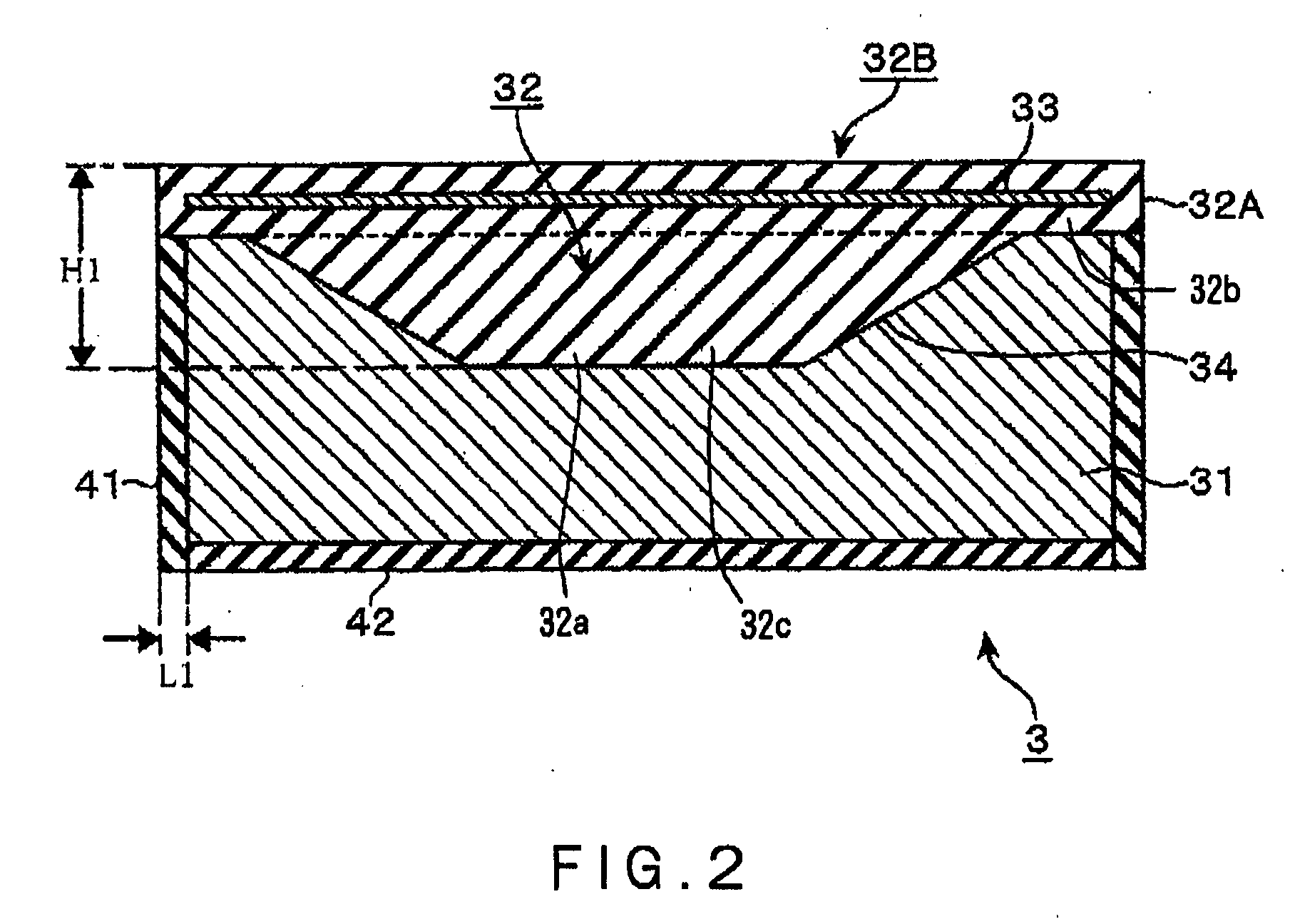
[0053]Next, the table 3 will be described in more detail with reference to FIG. 2. In a longitudinal side sectional view of the table 3 shown in FIG. 2, the coolant passage 42, back-side gas through-holes 43 and the like are omitted for convenience.

[0054]The lower electrode 31 has, for example, a circular shape, and its circumferential face is covered with the insulating member 41, as described above. The insulating member 41 is formed from, for example, alumite, or from ceramic formed by spraying. A thickness of the insulating member 41, as shown by L1 in the drawing, is, for example, 50 μm, in the case in which the insulating member 41 is formed of alumite, while, for example, several hundred microns, in the case in which it is formed of ceramic. The insulating member 42 covering the bottom face of the lower electrode 31 is composed of, for example, alumite.

[0055]In the top face of the lower electrode 31, an inverted frustum-shaped or cone-shaped recess 34 of a size smaller than t...

second embodiment

[0065]Next, a second embodiment of the table for use in the plasma processing apparatus 2 will be described with reference to FIG. 5. The table 6 shown in FIG. 5 includes the lower electrode 31 similar to that of the table 3 discussed above. In the top face of the lower electrode 31, the recess 37 as described above is provided. On the lower electrode 31, a first circular dielectric layer 61, which corresponds to the insulating material portion described in the above embodiment, is arranged for providing uniformity of the electron distribution density of the plasma over the wafer W. The dielectric layer 61 is fixedly attached onto the lower electrode 31 via an adhesive 62. The dielectric layer 61 includes a projection 61c, which projects downward to cover the whole top face of the lower electrode 31 and is formed such that its thickness becomes gradually greater as one moves from its peripheral portion 61b toward its central portion 61a. In this manner, the dielectric layer 61 is fi...

third embodiment

[0075]Next, a third embodiment of the table will be described with reference to FIG. 10(a). The table 8 includes the lower electrode 31 and the insulating members 41, 42, in the same manner as the table 3 of the first embodiment. However, the surface of the lower electrode 31 is not provided with the recess, but is formed to have a flat face. In addition, a flat column-like dielectric layer 81 is provided on the lower electrode 31 such that it covers the lower electrode 31. FIG. 10(b) is a view of the dielectric layer 81 when it is viewed from above. As shown in the drawing, the dielectric layer 81 is composed of a circular dielectric member 82 provided in a central portion, and annular dielectric members 83, 84 respectively provided to surround the dielectric member 82. The dielectric members 83, 84 have diameters different from each other, and are arranged concentrically with the center of the dielectric member 82, respectively. These dielectric members 82 to 84 are formed, by the...


PUM

PropertyMeasurementUnit
volume resistivityaaaaaaaaaa
frequencyaaaaaaaaaa
dielectric constantaaaaaaaaaa

Abstract

An object of the present invention is to suppress damage of an electrostatic chuck, by controlling stress exerted on each part of a table, which includes an electrically conductive material, i.e., an electrode for generating plasma, a dielectric layer for enhancing the in-plane uniformity of a plasma process, and an electrostatic chuck. The table for a plasma processing apparatus includes an electrically conductive member connected with a high frequency power source and adapted for plasma generation, for drawing ions present in the plasma, or for both thereof; a dielectric layer provided on a top face of the electrically conductive member, having a central portion and a peripheral portion that are different in thickness relative to each other, and adapted for providing uniformity of high frequency electric field intensity in a plane over the substrate to be processed; and an electrode film for an electrostatic chuck, provided in the dielectric layer and adapted for electrostatically chucking the substrate onto a top face of the dielectric layer. With such configuration, the stress exerted on the electrostatic chuck due to temperature change can be controlled.

Description

CROSS REFERENCE TO RELATED APPLICATIONS[0001]This application is based upon the prior Japanese Patent Application No. 2007-079717 filed on Mar. 26, 2007, and a provisional application U.S. 60 / 924,559 filed on May 21, 2007, the entire contents of which are incorporated herein by reference.BACKGROUND OF THE INVENTION[0002]1. Field of the Invention[0003]The present invention relates to a table for placing thereon a substrate to be processed, such as a semiconductor wafer or the like, to which a plasma process is provided, and a plasma processing apparatus including the table.[0004]2. Background Art[0005]Among steps of manufacturing semiconductor devices, there are many steps, in which a processing gas is changed into plasma, as in the case of dry etching, chemical vapor deposition (CVD), ashing and the like, so as to provide a process to each substrate. As the plasma processing apparatus for performing such a process, for example, an apparatus of a type, which includes a pair of parall...

Claims


Application Information

Patent Timeline
Patent Type & Authority Applications(United States)
IPC IPC(8): C23C16/00H01L21/306
CPCH01J37/32532H01L21/6831H01J2237/2001
Inventor HIGUMA, MASAKAZUHIMORI, SHLNJIMATSUYAMA, SHOICHIROMATSUURA, ATSUSHI
Owner TOKYO ELECTRON LTD
Why Eureka
Try Eureka