Plasma processing apparatus, plasma processing method and storage medium

a plasma processing and plasma technology, applied in the field of plasma processing apparatus, can solve the problems of exponential deterioration damage or destruction of insulating film, etc., to enhance the in-plane uniformity of plasma processing, prevent charging damage, and improve stability and reliability of plasma processing.

Inactive Publication Date: 2009-02-19
TOKYO ELECTRON LTD
View PDF27 Cites 26 Cited by
  • Summary
  • Abstract
  • Description
  • Claims
  • Application Information

AI Technical Summary

Benefits of technology

[0010]In view of the above, the present invention provides a plasma processing apparatus, method and a storage medium storing a control program for executing the plasma processing method for effectively preventing charging damage and improving stability and reliability of plasma processing and for enhancing the in-plane uniformity in the plasma processing.

Problems solved by technology

In general, the charging damage (dielectric breakdown) in the plasma processing depends on the amount of charges introduced or accumulated in the target object from the plasma and an insulating film is deteriorated or destroyed exponentially when the amount of the introduced or accumulated charges exceeds a threshold value.
In addition, the charge-up of the insulating film occurs due to unbalance between ions and electrons injected or introduced into the target object, thereby producing a local electric field.
Further, when the amount of charges exceeds the threshold value, the insulating film is damaged or destroyed.

Method used


Image

  • Plasma processing apparatus, plasma processing method and storage medium
  • Plasma processing apparatus, plasma processing method and storage medium
  • Plasma processing apparatus, plasma processing method and storage medium

Examples


Embodiment Construction

[0036]Embodiments of the present invention will be described with reference to the accompanying drawings which form a part hereof.

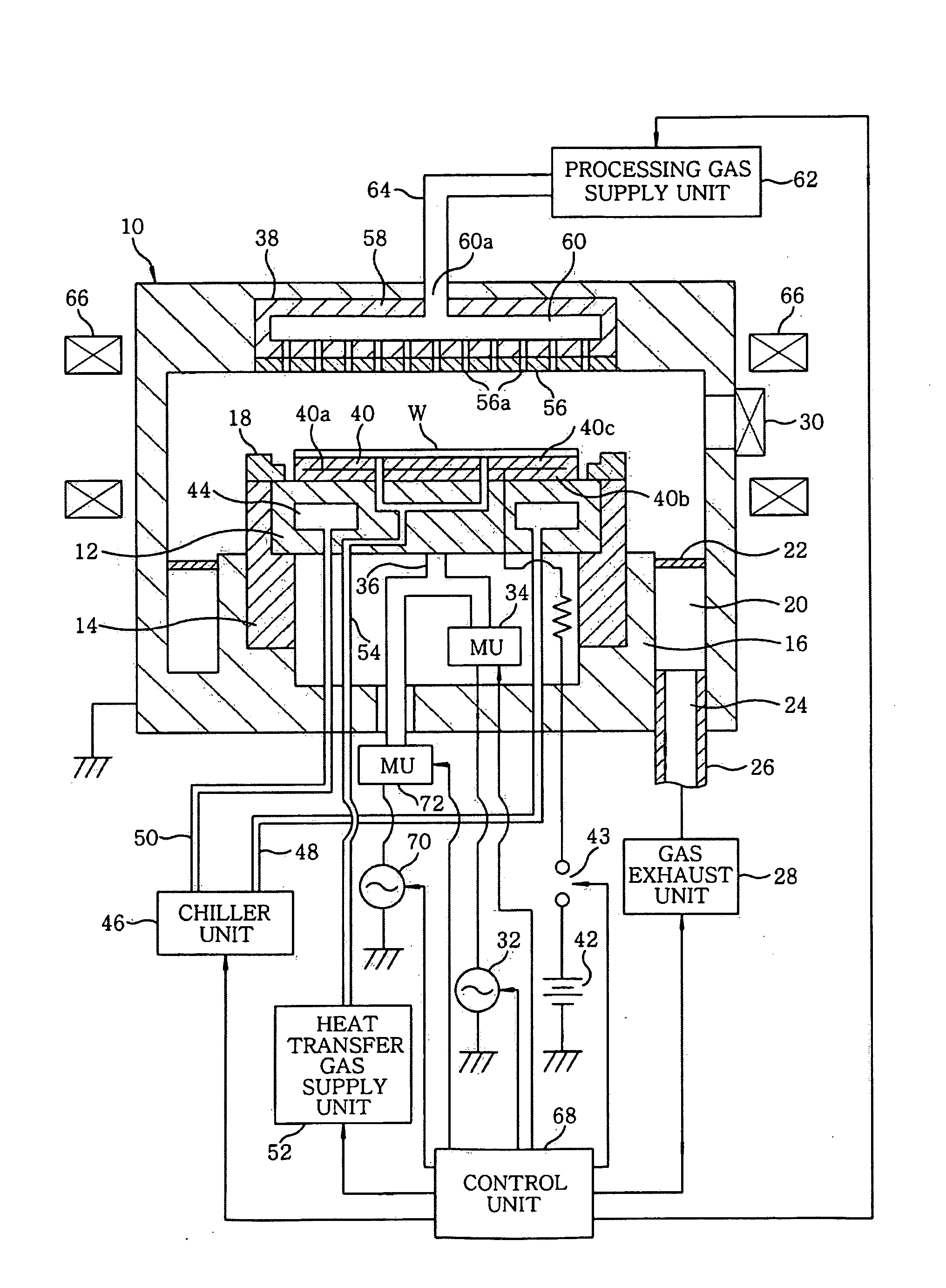
[0037]FIG. 1 shows a configuration of a plasma processing apparatus in accordance with an embodiment of the present invention. The plasma processing apparatus is configured as a capacitively coupled (parallel plate type) plasma etching apparatus wherein dual RF frequency powers are applied to a lower electrode, and has a cylindrical chamber (processing chamber) 10 made of a metal such as aluminum, stainless steel or the like. The chamber 10 is frame grounded.

[0038]A circular plate-shaped lower electrode or susceptor 12 for mounting thereon a target object (a substrate to be processed), e.g., a semiconductor wafer W, is installed in the chamber 10. The susceptor 12 is made of, e.g., aluminum, and is supported by a cylindrical support 16 vertically extended from a bottom of the chamber 10 via an cylindrical insulating member 14. On the top surface of the cy...


PUM

PropertyMeasurementUnit
frequencyaaaaaaaaaa
frequencyaaaaaaaaaa
frequencyaaaaaaaaaa

Abstract

A plasma processing apparatus includes a first radio frequency (RF) power supply unit for applying a first RF power for generating a plasma from a processing gas to at least one of a first and a second electrode which are disposed facing each other in an evacuable processing chamber. The first RF power supply unit is controlled by a control unit so that a first phase at which the first RF power has a first amplitude for generating a plasma and a second phase at which the first RF power has a second amplitude for generating substantially no plasma are alternately repeated at predetermined intervals.

Description

FIELD OF THE INVENTION[0001]The present invention relates to a technique for performing plasma processing on a target object; and, more particularly, to a capacitively coupled plasma processing apparatus, a plasma processing method and a storage medium storing a control program for executing the plasma processing method.BACKGROUND OF THE INVENTION[0002]In a manufacturing process of a semiconductor device or an FPD (flat panel display), a plasma is often used in processes, e.g., etching, deposition, oxidation, sputtering and the like, in order to allow a processing gas to react efficiently at a relatively low temperature. Conventionally, a capacitively coupled plasma processing apparatus is mainly used for a single-wafer plasma processing apparatus, especially a single-wafer plasma etching apparatus.[0003]Generally, in the capacitively coupled plasma processing apparatus, an upper and a lower electrode are disposed in parallel with each other in a processing chamber as a vacuum chamb...

Claims


Application Information

Patent Timeline
Patent Type & Authority Applications(United States)
IPC IPC(8): H01L21/306H01L21/3065H01L21/31
CPCH01J37/32091H01L21/3065H01J37/32165H01J37/32146
Inventor MATSUDO, TATSUOHIMORI, SHINJIIMAI, NORIAKIOHSE, TAKESHIABE, JUNKATSUNUMA, TAKAYUKI
Owner TOKYO ELECTRON LTD
Why Eureka
Try Eureka