Electrostatic chuck device

Active Publication Date: 2008-03-13
TOKYO ELECTRON LTD +1
View PDF10 Cites 26 Cited by
  • Summary
  • Abstract
  • Description
  • Claims
  • Application Information

AI Technical Summary

Benefits of technology

[0057] As described above, when the conductive adhesive bonding layer includes a silicon-based adhesive bonding agent containing a conductive filler or a metal-based adhesive bonding agent, it is possible to easily adjust the volume resistivity of the conductive adhesive bonding agent to 1.0×10⁻²Ωcm or less.
[0058] As described above, the electrostatic-adsorption inner electrode includes a plurality of concentric electrode portions electrically isolated from each other and the power supply terminals are connected to the electrode portions, respectively. In this state, when a high-frequency voltage is applied, it is possible to effectively prevent a high-frequency current from flowing toward the outer peripheral edge through the electrostat

Problems solved by technology

Therefore, there is a problem in that it is not possible to

Method used


Image

  • Electrostatic chuck device
  • Electrostatic chuck device
  • Electrostatic chuck device

Examples


first embodiment

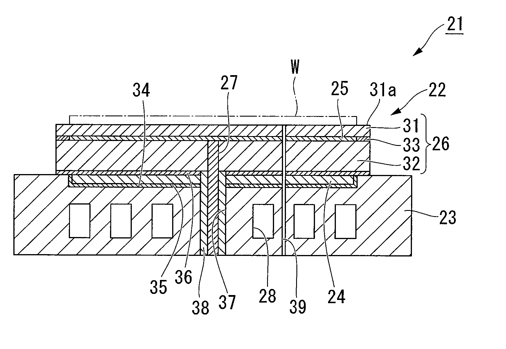
[0073]FIG. 1 is a cross-sectional view illustrating a unipolar electrostatic chuck device 21 according to a first embodiment of the invention. The electrostatic chuck device 21 includes an electrostatic chuck section 22, a metal base section 23, and a dielectric plate 24.

[0074] The electrostatic chuck section 22 includes a disc-like substrate 26, the top surface (one main surface) of which serves as a mounting surface for mounting a plate-like sample W and in which an electrostatic-adsorption inner electrode 25 is built, and a power supply terminal 27 for applying a DC voltage to the electrostatic-adsorption inner electrode 25.

[0075] The substrate 26 roughly includes a disc-like mounting plate 31 of which the top surface 31a serves as the mounting surface for mounting the plate-like sample W such as a semiconductor wafer, a metal wafer, and a glass plate, a disc-like support plate 32 disposed opposite the bottom surface (the other main surface) of the mounting plate 31, a circular...

second embodiment

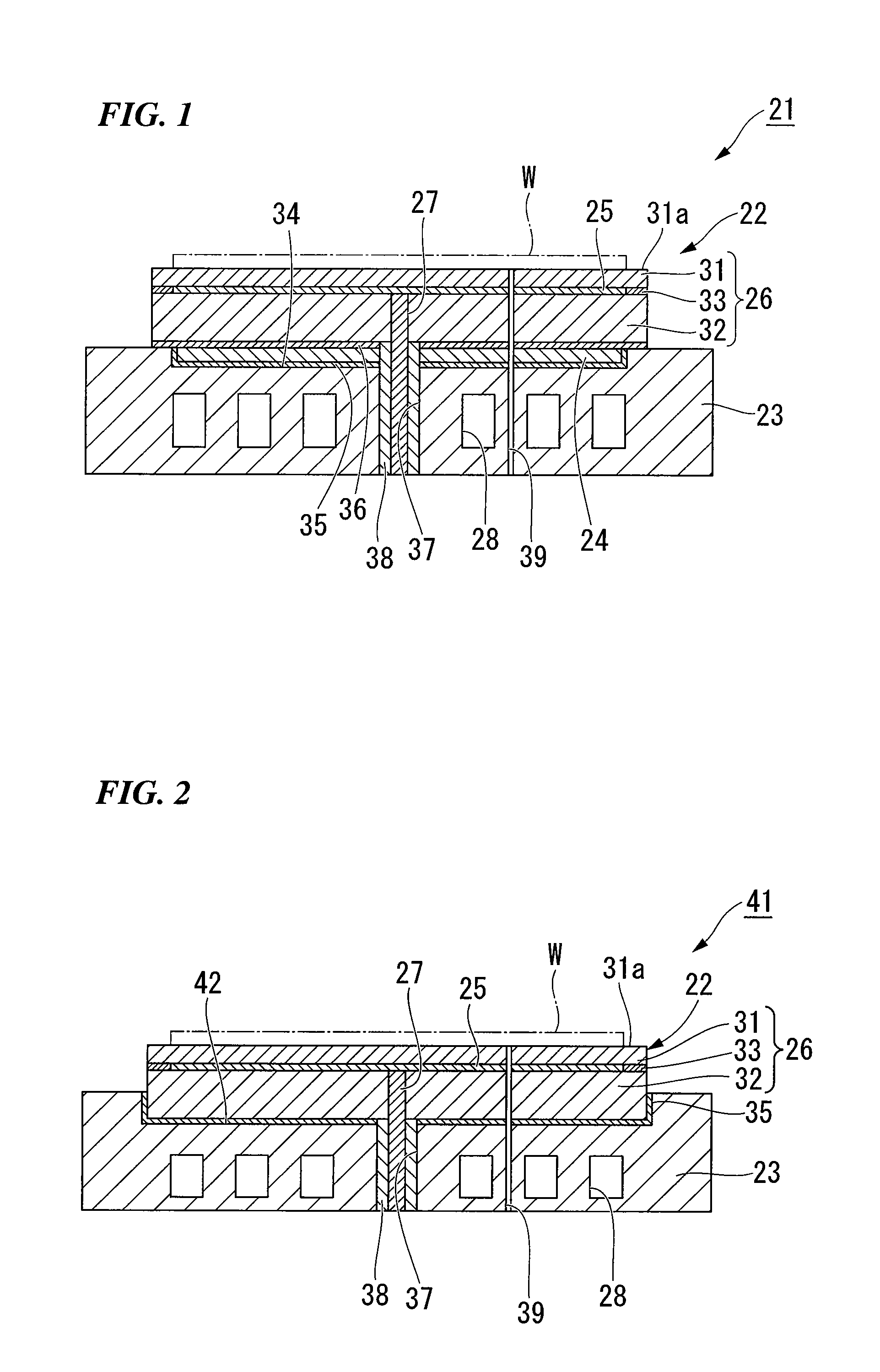
[0155]FIG. 2 is a cross-sectional view illustrating an electrostatic chuck device 41 according to a second embodiment of the invention. The electrostatic chuck device 41 according to the second embodiment is different from the electrostatic chuck device 21 according to the first embodiment, in that a concave portion 42 having the same shape as the bottom surface of the electrostatic chuck section 22 and having a height smaller than the height of the electrostatic chuck section 22 is formed in a surface (main surface) of the metal base section 23 facing the electrostatic chuck section 22 and the support plate 32 of the electrostatic chuck section 22 is adhesively bonded to the concave portion 42 with the conductive adhesive bonding layer 35 interposed therebetween, the volume resistivity of which at the usage temperature of the electrostatic chuck device is 1.0×10⁻²Ωcm or less.

[0156] In the electrostatic chuck device 41, the electrostatic chuck section 22 and the concave portion 42 ...

third embodiment

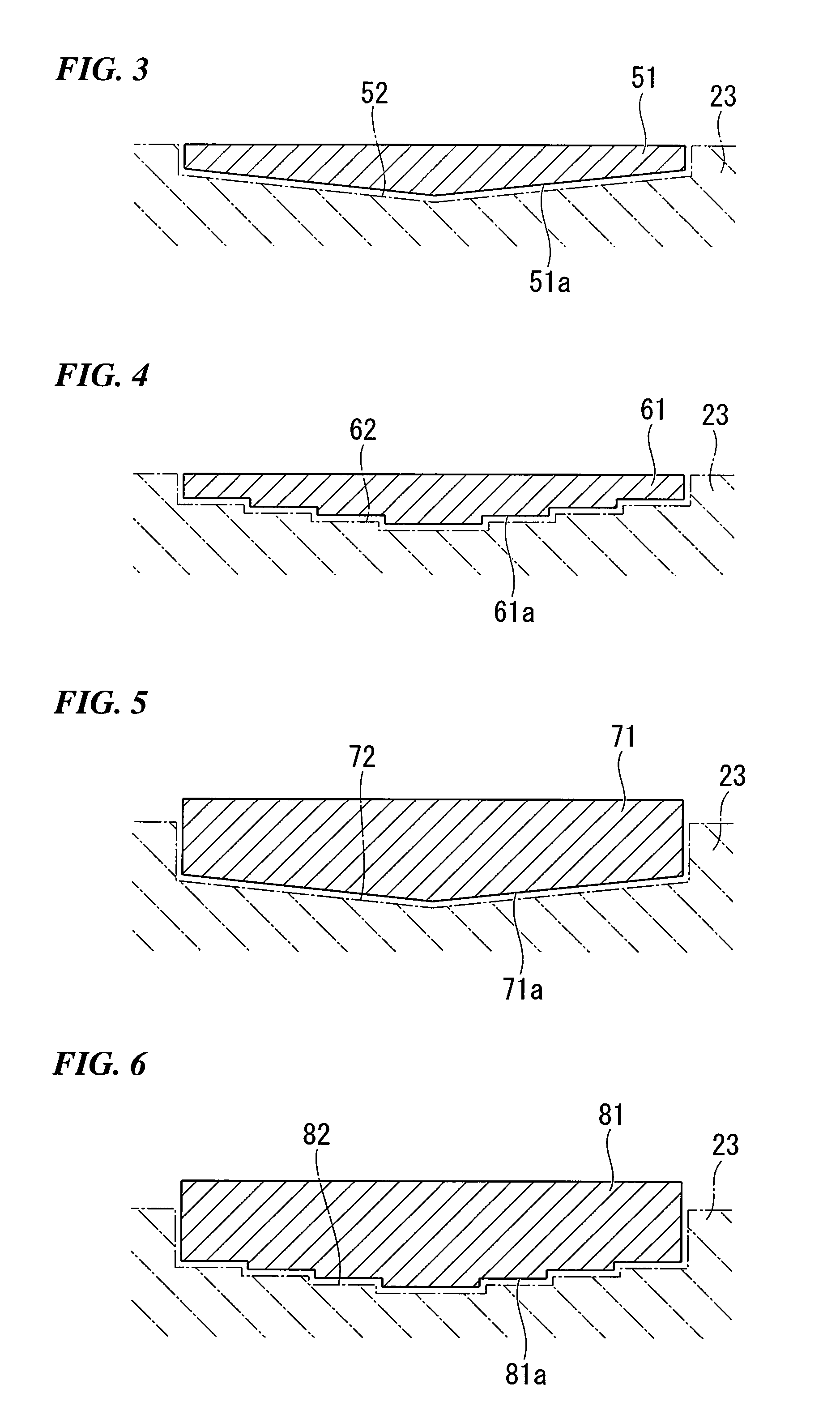
[0164]FIG. 3 is a cross-sectional view illustrating a dielectric plate 51 of an electrostatic chuck device according to a third embodiment of the invention. The dielectric plate 51 according to the third embodiment is different from the dielectric plate 24 according to the first embodiment, in that a bottom surface 51a of the dielectric plate 51 is formed in a cone shape so that the thickness of the dielectric plate 51 concentrically and gradually decreases from the center to the peripheral edge thereof.

[0165] When the dielectric plate 51 is employed, it is possible to easily and satisfactorily position and fix the metal base section 23 and the dielectric plate 51 relative to each other, by forming a concave portion 52, which has a shape complementary to the bottom surface 51a of the dielectric plate 51, in the metal base section 23.

[0166] In the dielectric plate 51 according to this embodiment, since the thickness thereof concentrically and gradually decreases from the center to ...


PUM


Abstract

An electrostatic chuck device includes an electrostatic chuck section, a metal base section, and a dielectric plate. The electrostatic chuck section has a substrate, a main surface of which serves as a mounting surface for a plate-like sample, an electrostatic-adsorption inner electrode built in the substrate, and a power supply terminal for applying a DC voltage to the electrostatic-adsorption inner electrode. Here, a dielectric plate is fixed to a concave portion formed in the metal base section. The dielectric plate and the electrostatic chuck section are adhesively bonded to each other with an insulating adhesive bonding layer interposed therebetween. The dielectric plate and the concave portion are adhesively bonded to each other with a conductive adhesive bonding layer interposed therebetween, the volume resistivity of which is 1.0×10⁻²Ωcm or less.

Description

BACKGROUND OF THE INVENTION [0001] 1. Field of the Invention [0002] The present invention relates to an electrostatic chuck device, and more particularly, to an electrostatic chuck device suitable for use in a high-frequency discharge type plasma processing apparatus for applying a high-frequency voltage to an electrode to generate plasma and processing a plate-like sample such as a semiconductor wafer, a metal wafer, and a glass plate by the use of the generated plasma. [0003] Priority is claimed on Japanese Application No. 2006-218447, filed Aug. 10, 2006, which is incorporated herein by reference. This application also claims the benefit pursuant to 35 U.S.C. §102(e) of U.S. Provisional Application No. 60 / 828,405, filed on Oct. 6, 2006. [0004] 2. Description of the Related Art [0005] Conventionally, plasma was often used in processes such as etching, deposition, oxidation, and sputtering for manufacturing semiconductor devices such as IC, LSI, and VLSI or flat panel displays (FPD...

Claims


Application Information

Patent Timeline
IPC IPC(8): H01L21/683
CPCH01L21/6833
Inventor HIMORI, SHINJIMATSUYAMA, SHOICHIROMATSUURA, ATSUSHIINAZUMACHI, HIROSHIKOSAKAI, MAMORUMIURA, YUKIOMAKI, KEIGO
Owner TOKYO ELECTRON LTD
Why Eureka
Try Eureka