Force deflection and resistance testing system and method of use
a technology of force deflection and resistance, applied in the field of testing systems, can solve the problems of inability to test a plurality of electrical interconnects in conventional testing systems, inability to easily convert conventional testing systems between configurations, and extremely limited cleanroom space, so as to reduce the space needed in the cleanroom, quick and easy removal and replacement, the effect of reducing the cost of capital equipmen
Active Publication Date: 2017-07-06
MODUS TEST
View PDF3 Cites 2 Cited by
- Summary
- Abstract
- Description
- Claims
- Application Information
AI Technical Summary
Benefits of technology
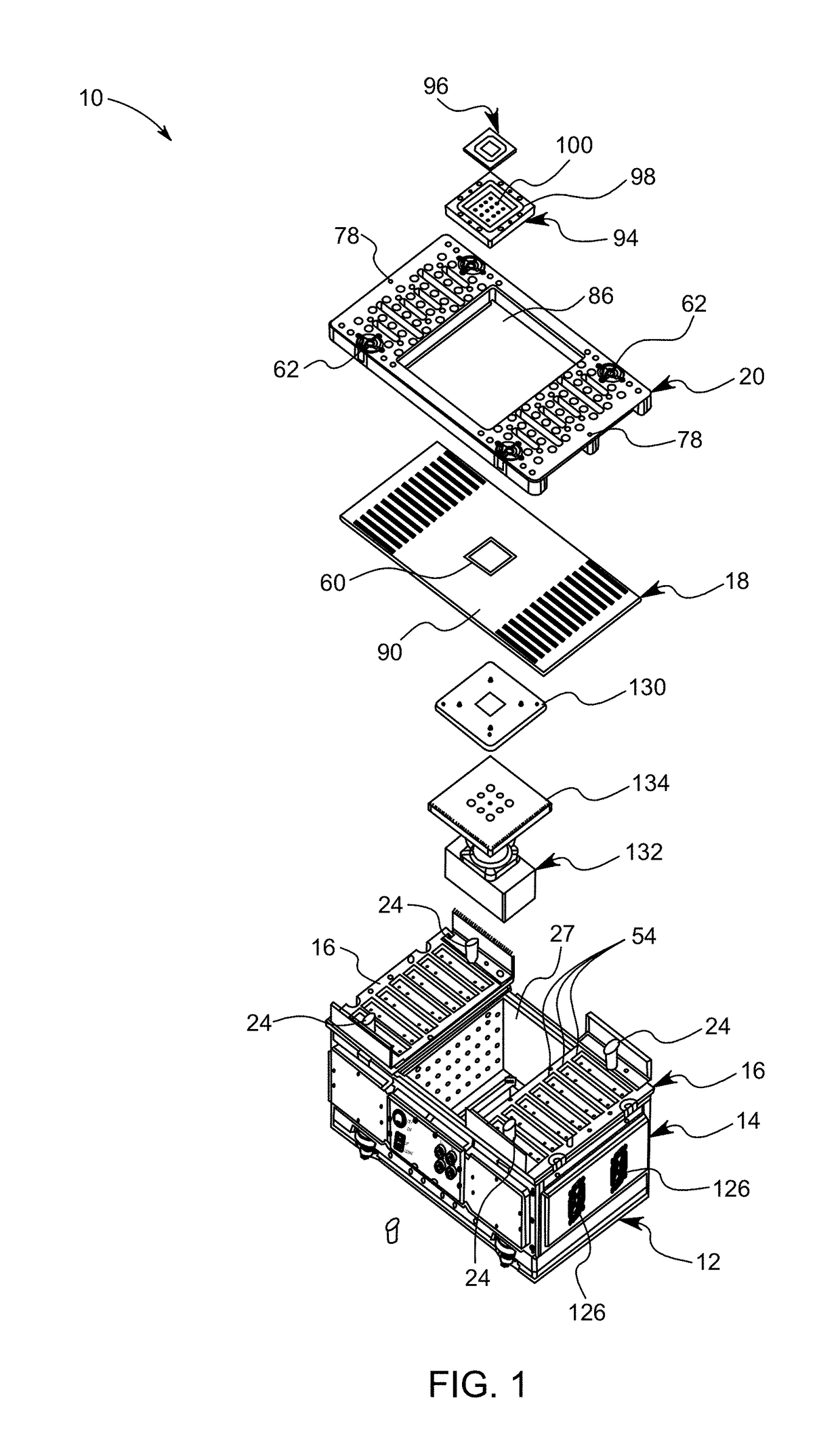
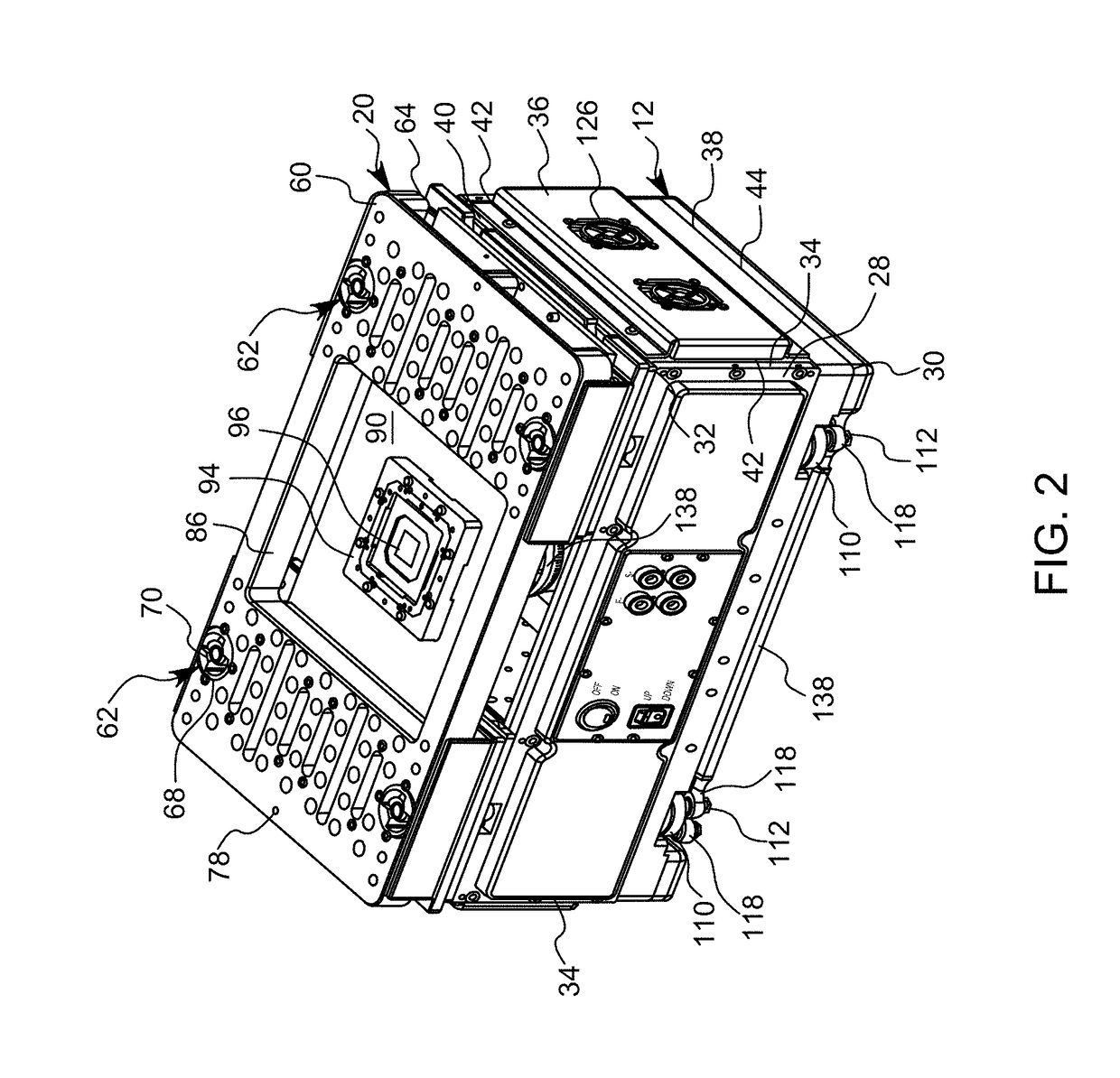
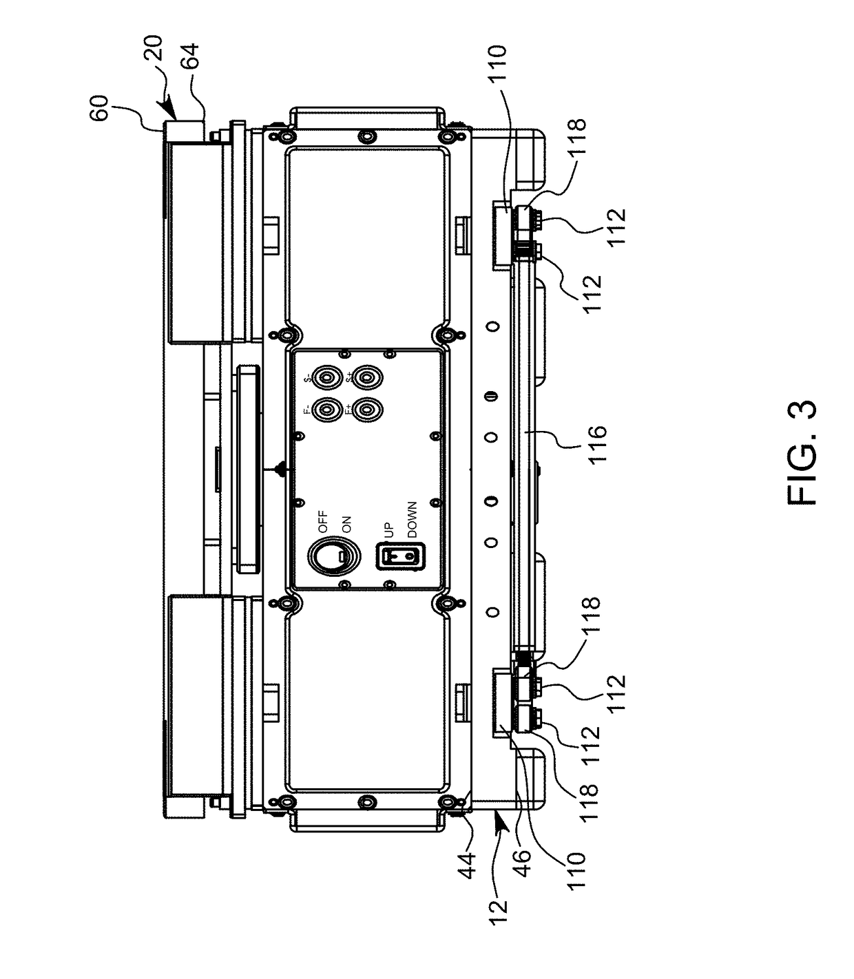
[0023]A testing system is presented having a bottom plate, a frame member and a socket plate. The socket plate holds and the frame member houses a plurality of electrical testing components therein. A removable device under test (DUT) printed circuit board (PCB) is placed on top of the socket plate and electrically connects with the electrical testing components. A removable top plate is placed on top of the DUT PCB and is locked in place by a plurality of locking posts connected to an actuating mechanism. The locking posts connect to cam surfaces in the top plate that selectively hold the top plate in place thereby sandwiching the DUT PCB between the
Problems solved by technology
The DUT PCB and electrical interconnects are generally custom made to fit each specific semiconductor chip, making them quite expensive.
Since cleanroom space is extremely limited it is undesirable to have a dedicated testing machine for each type
Method used
View moreImage
Smart ImageViewing Examples

Examples
 PUM
 Abstract
A testing system for electrical interconnects having a removable device under test printed circuit board (DUT PCB) that electrically connects with the electrical testing components of the system. A removable top plate is placed on top of the DUT PCB and is locked in place by a plurality of locking posts that selectively connect to cam surfaces in the top plate that pull the top plate down sandwiching the DUT PCB between the top plate and the electrical testing components of the system. An actuator is also presented that presses the device under test into the electrical interconnect at increments where tests are performed on one, some or all of the contact points of the electrical interconnect. This information is then analyzed and graphed to assist with determine the optimum force and/or height to use during actual use.
Description
CROSS-REFERENCE TO RELATED APPLICATIONS[0001]The present application is a continuation-in-part of U.S. patent application Ser. No. 14 / 996,045 which was filed on Jan. 14, 2016, which claims priority to U.S. Provisional Patent Application No. 62 / 104,117 which was filed on Jan. 16, 2015, which is hereby incorporated by reference herein in its entirety, including any figures, tables, or drawings.FIELD OF THE DISCLOSURE[0002]This disclosure relates to a testing system. More specifically and without limitation, this disclosure relates to a testing system for electrical interconnects, and related method of use.BACKGROUND OF THE DISCLOSURE[0003]Along with the development of semiconductor chips, a need developed to test these semiconductor chips to ensure that they are manufactured within specified tolerances and function properly. Many manufacturers of semiconductor chips such as Intel®, AMD®, Xilinx®, Texas Instruments®, NVIDIA®, Qualcomm® among countless others manufacture semiconductor c...
Claims
Login to View More Application Information
Patent Timeline
 IPC IPC(8): G01R31/04
CPCG01R31/043G01R1/0466G01R1/07328G01R31/2879G01R31/2889G01R1/07314G01R31/2886G01R31/2896G01R31/69G01R31/66G01R31/54G01R31/52G01R31/67G01R31/50
Inventor ADAMS, LYNWOODLEWIS, JACK
Owner MODUS TEST