Method for manufacturing memory device

a memory device and manufacturing method technology, applied in the direction of basic electric elements, semiconductor devices, electrical apparatus, etc., can solve the problems of unsatisfactory performance and/or quality of the memory device, affecting the performance of the floating gate, and not being substantially removed, so as to achieve satisfactory reliability and/or performance of the electromechanical device, and the floating gate performance. satisfactory

Active Publication Date: 2017-07-06
SEMICON MFG INT (SHANGHAI) CORP +1
View PDF4 Cites 3 Cited by
  • Summary
  • Abstract
  • Description
  • Claims
  • Application Information

AI Technical Summary

Benefits of technology

[0019]According to embodiments, in manufacturing of a memory device, unwanted insulating material portions (e.g., oxide portions) that have attached to sidewalls of floating gates (e.g., side walls of the first conductor and / or the second conductor) of the memory device may be effectively removed. As a result, satisfactory performance of the floating gates may be attained. Advantageously, satisfactory reliability and / or performance of the electromechanical device may be attained.

Problems solved by technology

In manufacturing of the memory device, after the STI members have been formed, some unwanted insulating material portions (e.g., oxide portions) may remain on sidewalls of the floating gates and may not be substantially removed.
The remaining insulating material portions may negatively affect performance of the floating gates.
As a result, performance and / or quality of the memory device may be unsatisfactory.

Method used


Image

  • Method for manufacturing memory device
  • Method for manufacturing memory device
  • Method for manufacturing memory device

Examples


Embodiment Construction

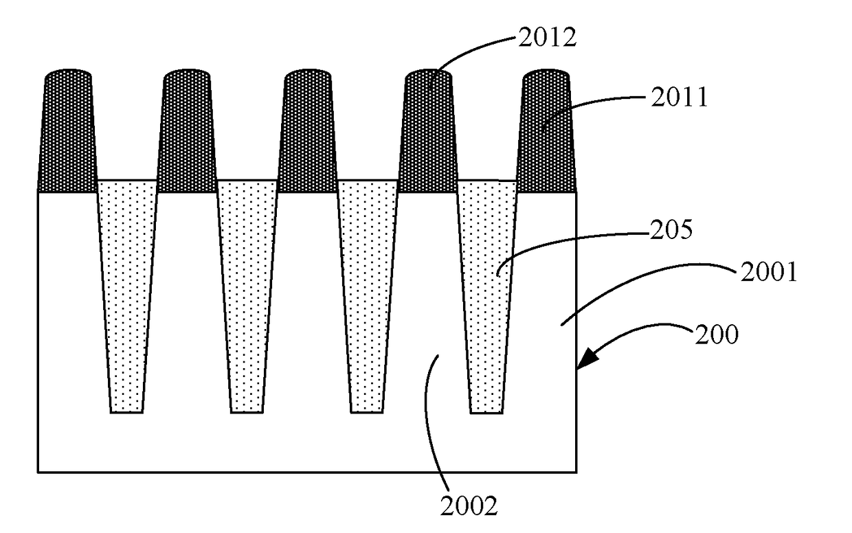
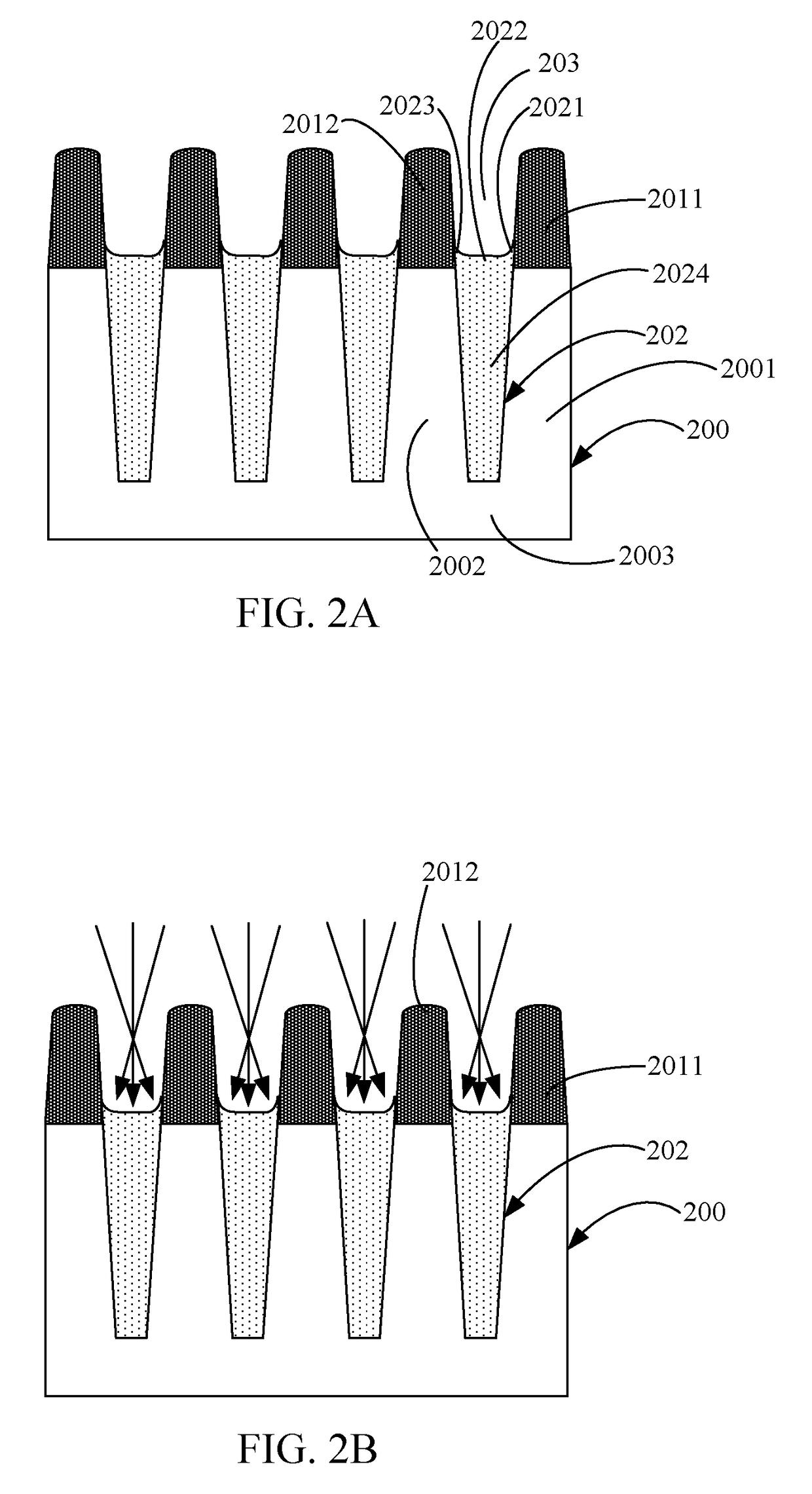
[0023]Example embodiments are described with reference to the accompanying drawings. As those skilled in the art would realize, the described embodiments may be modified in various different ways, all without departing from the spirit or scope. Embodiments may be practiced without some or all of these specific details. Well known process steps and / or structures may not have been described in detail in order to not unnecessarily obscure described embodiments.

[0024]The drawings and description are illustrative and not restrictive. Like reference numerals may designate like (e.g., analogous or identical) elements in the specification. Repetition of description may be avoided.

[0025]The relative sizes and thicknesses of elements shown in the drawings are for facilitate description and understanding, without limiting possible embodiments. In the drawings, the thicknesses of some layers, films, panels, regions, etc., may be exaggerated for clarity.

[0026]Illustrations of example embodiments...


PUM


Abstract

A method for manufacturing a memory device may include the following steps: preparing a first semiconductor, a second semiconductor, a first conductor, and a second conductor, wherein the second semiconductor is spaced from the first semiconductor, wherein the first conductor directly contacts the first semiconductor, and wherein the second conductor is spaced from the first conducive member and directly contacts the second semiconductor; preparing a dielectric material member, which is positioned between the first semiconductor and the second semiconductor and directly contacts each of the first semiconductor, the second semiconductor, the first conductor, and the second conductor; performing ion implantation on the dielectric material member to form an implanted member and a dielectric member; and removing the implanted member.

Description

CROSS-REFERENCE TO RELATED APPLICATION[0001]This application claims priority to and benefit of Chinese Patent Application No. 201610006426.7, filed on 6 Jan. 2016; the Chinese Patent Application is incorporated herein by reference in its entirety.BACKGROUND OF THE INVENTION[0002]The technical field is related to a method for manufacturing a memory device, such as a flash memory device, e.g., a NAND memory device.[0003]A memory device may be used in write operations for storing data and may be used in read operations for retrieving data. A memory device may include floating gates and shallow trench isolation (STI) members positioned between the floating gates.[0004]In manufacturing of the memory device, after the STI members have been formed, some unwanted insulating material portions (e.g., oxide portions) may remain on sidewalls of the floating gates and may not be substantially removed. The remaining insulating material portions may negatively affect performance of the floating ga...

Claims


Application Information

Patent Timeline
Patent Type & Authority Applications(United States)
IPC IPC(8): H01L21/762H01L27/115H01L29/06H01L21/3115H01L21/311
CPCH01L21/762H01L21/31155H01L27/11521H01L29/0649H01L21/31111H10B41/00H01L21/823481H01L21/823878H01L21/76224H01L21/76237H01L29/785H10B41/30H01L21/76
Inventor CHEN, LIANG
Owner SEMICON MFG INT (SHANGHAI) CORP
Why Eureka
Try Eureka