

Optical element holding apparatus
a technology of holding apparatus and optical element, which is applied in the direction of photomechanical apparatus, instruments, optical elements, etc., can solve the problems of increasing manufacturing costs, extremely low wave front aberration and distortion, and troublesome individual member machining, etc., and achieve the effect of maintaining the optical performance of an optical elemen
- Summary
- Abstract
- Description
- Claims
- Application Information
AI Technical Summary
Benefits of technology
Problems solved by technology
Method used
Image

Examples
first embodiment
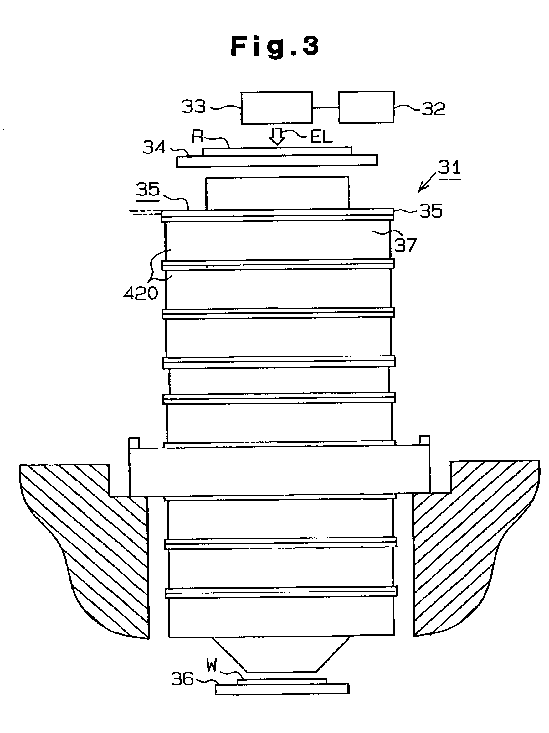
[0066]An optical element holding apparatus 39 according to a first embodiment of the present invention will now be described with reference to FIGS. 3 through 19. Referring to FIG. 3, the optical element holding apparatus 39 is used to hold an optical element or a lens 38 of a projection optical system 35 of an exposure apparatus 31 that is used in the fabrication of semiconductor devices.
[0067]As shown in FIG. 3, the exposure apparatus 31 includes a light source 32, an illumination optical system 33, a reticle stage 34, which holds a reticle R functioning as a mask, a projection optical system 35, and a wafer stage 36, which holds a wafer W functioning as a substrate.
[0068]The light source 32 emits, for example, an ArF excimer laser beam having a wavelength of, for example, 193 nm. The illumination optical system 33 various lens systems, for example, an optical integrator, such as a fly-eye lens or a rod lens, a relay lens, and a condenser lens, and an aperture stop, which are not ...
second embodiment
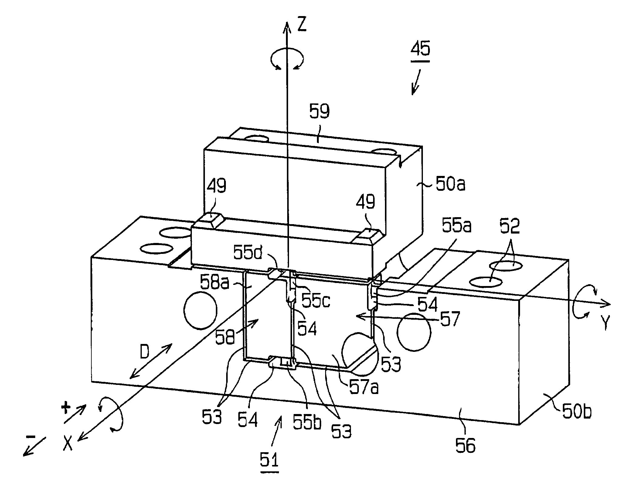
[0127]An optical element holding apparatus 39 according to a second embodiment of the invention will be described below, centering on the differences from the first embodiment.
[0128]In the second embodiment, as shown in FIGS. 21 to 23, a bearing surface 91 of the bearing surface block 50a and an action surface 92 of the pad member 47 are formed extending in the tangential direction of the optical element 38.
[0129]A housing hole 93 is formed in the centers of the bearing surface 91 and the action surface 92. A contractible adhesive which volume slightly contracts when hardening is charged in the housing hole 93. The flange portion 38a of the optical element 38 is connected to the bearing surface 91 and the action surface 92 by the adhesive charged in the housing hole 93. An adhesive charging hole 94 which is connected to the housing hole 93 may be formed in the bottom of the housing hole 93 as shown by the broken lines in FIG. 22.
[0130]The optical element holding apparatus 39 of the ...
third embodiment
[0140]An optical element holding apparatus 139 according to a third embodiment of the present invention will be described below with reference to the accompanying drawings.
[0141]FIG. 23 is a perspective view of the optical element holding apparatus 139, FIG. 24 is a plan view of the optical element holding apparatus 139, FIG. 25 is a side view of the optical element holding apparatus 139, and FIG. 26 is a cross-sectional view taken along the line 26—26 in FIG. 25. The optical element holding apparatus 139 includes a frame 142, three flexure members 41, a lens frame 40, and holders 43. The three flexure members 41 are fixed to the frame 142 at equiangular distances. The lens frame 40 is fixed to the top surfaces of the flexure members 41, and the three holders 43 are provided on the lens frame 40 at equiangular distances.
[0142]The structure of the lens frame 40 is similar to that of the lens frame 42 of the optical element holding apparatus 39 discussed in the first and second embodi...
PUM
| Property | Measurement | Unit |
|---|---|---|
| wavelength | aaaaa | aaaaa |
| thickness | aaaaa | aaaaa |
| thickness | aaaaa | aaaaa |
Abstract
Description
Claims
Application Information