Three-dimensional hybrid packaging with through-silicon-vias and tape-automated-bonding

a technology of silicon-via and tape, applied in the direction of semiconductor devices, semiconductor/solid-state device details, electrical apparatus, etc., can solve the problems of ic chips with tsvs, wire bonds typically have a higher resistance and signal transmission bandwidth, and it is difficult to obtain low-cost, high-performance electrical connections between stacked ic chips

Active Publication Date: 2017-07-13
GLOBALFOUNDRIES US INC
View PDF0 Cites 7 Cited by
  • Summary
  • Abstract
  • Description
  • Claims
  • Application Information

AI Technical Summary

Problems solved by technology

It can, however, be difficult to obtain low-cost, high-performance electrical connections between stacked IC chips.
But while these wire bonds can be implemented using low-cost assembly techniques, the resulting wire bonds typically have a higher resistance and lower bandwidth for signal transmission due to their length.
However, a disadvantage of stacked IC chips with TSVs can include the large number of TSVs required for the transmission of I / 0 signals from the topmost chip or an upper level chip to the underlying laminate base or a lower level chip that requires a pathway of TSVs through all of the intervening chips.
In addition, the efficient distribution of power / ground to upper level chips from the underlying laminate base also suffers from transmission losses through the pathways of TSVs, each of which includes the TSVs of each of the intervening chips in the stack.

Method used


Image

  • Three-dimensional hybrid packaging with through-silicon-vias and tape-automated-bonding
  • Three-dimensional hybrid packaging with through-silicon-vias and tape-automated-bonding
  • Three-dimensional hybrid packaging with through-silicon-vias and tape-automated-bonding

Examples


Embodiment Construction

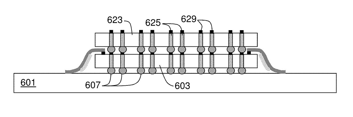
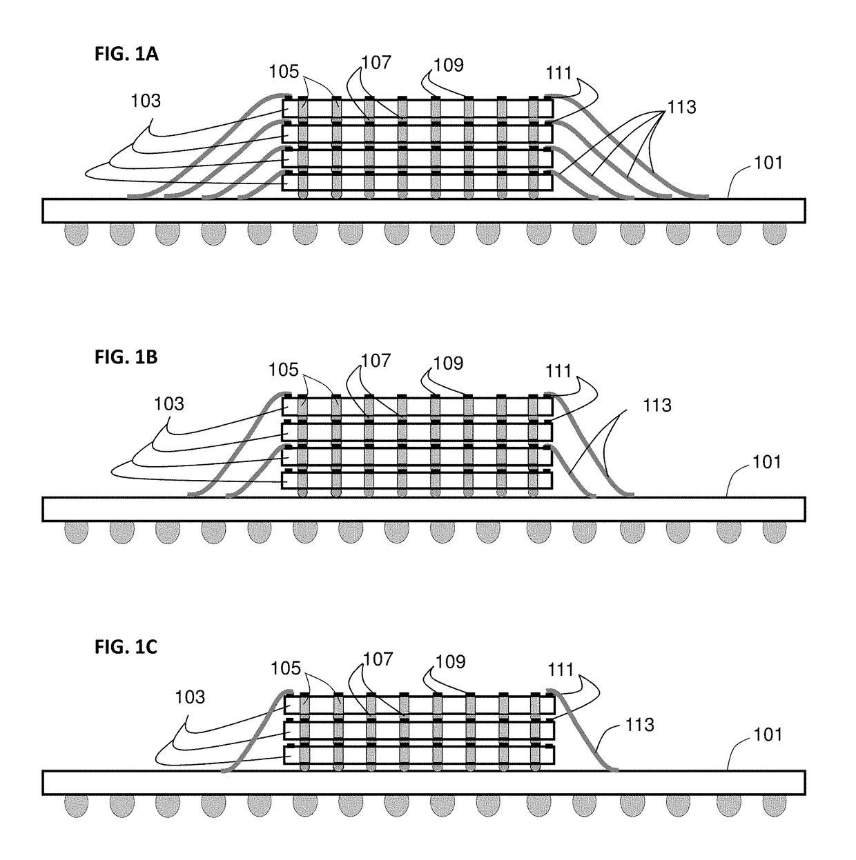
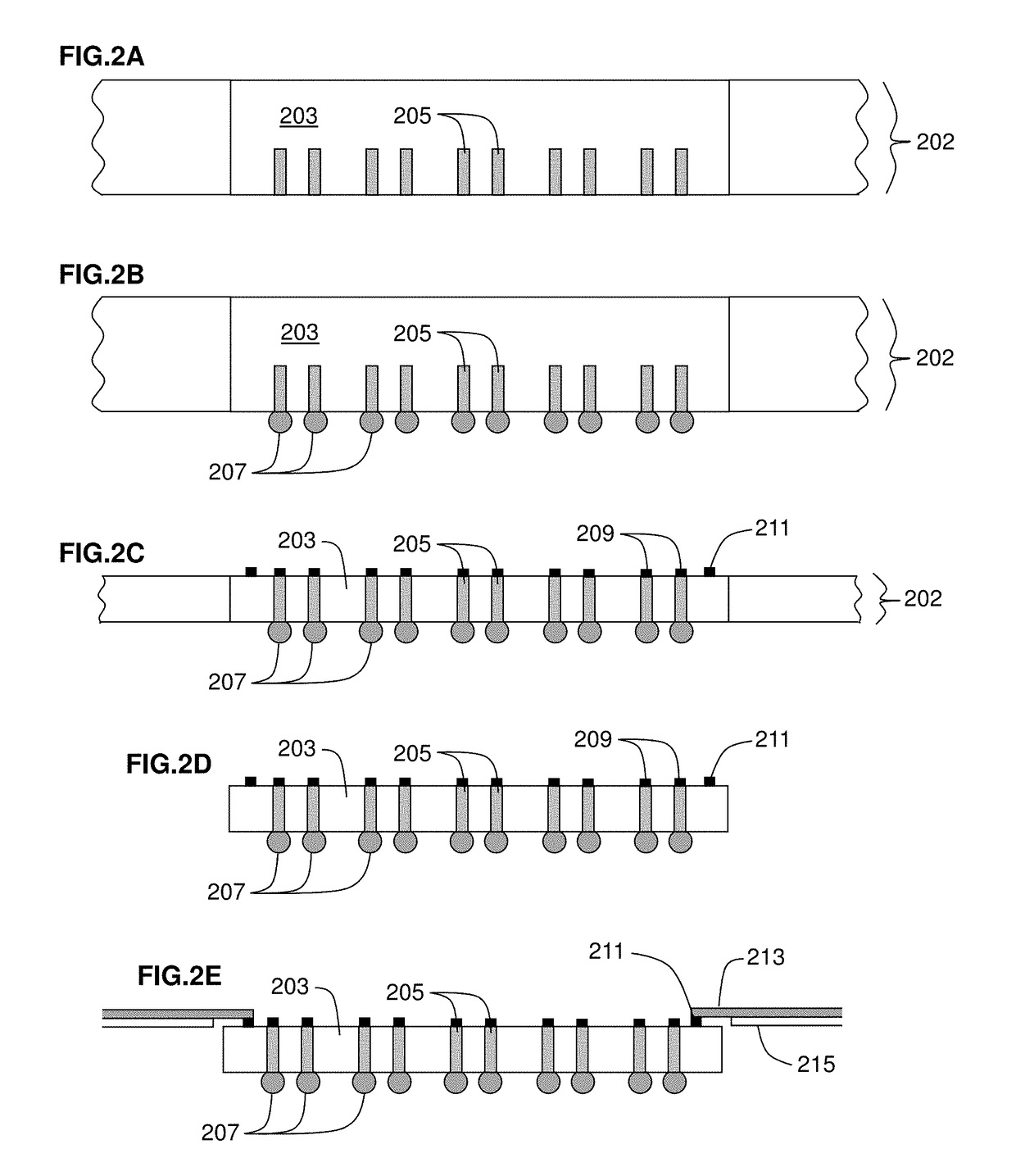
[0034]As stated above, there remains a need for a three-dimensional (3D) package including multiple integrated circuit (IC) chips, stacked one atop the other, on a laminate that provides a more efficient distribution of signals and of power / ground between all levels of a chip stack and of a laminate base.

[0035]Referring to the exemplary embodiments illustrated in FIGS. 1A-C, a 3D hybrid package may include multiple IC chips 103, stacked one atop the other, on a laminate 101. Each of the IC chips 103 in the stack is flipped and includes through-silicon-vias (TSVs) 105 that extend through the silicon from the front side to the back side of the IC chip. Upon each of the TSVs 105, solder bumps 107 are formed on the front side of each of the IC chips 103, while more centrally-located metal pads 109 are formed on the back side of each TSV 105 of each IC chip 103. The solder bumps 105 may include a solder further including of any of tin and lead, lead-free tin alloys yet further including ...


PUM


Abstract

A 3-dimensional hybrid package including an integrated circuit chip stack formed on a laminate, the integrated chip stack further including a first chip and a second chip. The first chip is connected to the laminate through first solder bumps, each associated with a first through-silicon via (TSV), and first metal leads embedded in a first polymer tape that extends from first peripheral metal pads formed on a back side of the first chip to the laminate. The second chip is connected to the first peripheral metal pads on the back side of the first chip through second solder bumps formed on a front side of the second chip. The second chip is connected to the laminate by second metal leads, embedded in a second polymer tape that extend from second peripheral metal pads formed on a back side of the second chip to the laminate.

Description

BACKGROUND[0001]Field of the Invention[0002]The present disclosure generally relates to a three-dimensional (3D) package including multiple integrated circuit (IC) chips, stacked one atop the other, on a laminate and a method of fabricating a hybrid 3D package including the hybrid processes of forming through-silicon-vias (TSVs) in each stacked IC chip and of tape automated bonding (TAB) from at least one stacked chip to the laminate.[0003]Description of Related Art[0004]A three-dimensional (3D) package contains two or more integrated circuit (IC) chips stacked vertically, so as to occupy less space and provide greater connectivity between IC chips. It can, however, be difficult to obtain low-cost, high-performance electrical connections between stacked IC chips. For example, IC chips can be electrically coupled using wire bonds between exposed bond pads on surfaces of a stack of chips, in which the chips are offset from one another to define a staircase of chip edges. But while the...

Claims


Application Information

Patent Timeline
Patent Type & Authority Applications(United States)
IPC IPC(8): H01L25/065H01L25/00
CPCH01L25/0657H01L25/50H01L2225/06579H01L2225/06513H01L2225/06541H01L24/50H01L2224/13025H01L2224/16145H01L2224/16227H01L2224/17181H01L2224/50H01L2224/73261H01L2225/06517H01L2924/15311H01L2225/06565H01L24/86H01L23/48H01L23/482H01L23/495H01L25/00H01L25/065H01L29/40H01L29/41
Inventor GRAF, RICHARD S.VENTRONE, SEBASTIAN T.
Owner GLOBALFOUNDRIES US INC
Why Eureka
Try Eureka