

Ion-assisted deposition and implantation of photoresist to improve line edge roughness
a technology of photoresist and ion-assisted deposition, which is applied in the field of substrate patterning, can solve the problems of reducing the chemical structure of the resist through plasma chemistries and direct physical sputtering, reducing the volume of the photoresist, and difficult modification of the resist without removal, so as to reduce a certain amount of ler and improve the structure of the resist. , the effect of reducing the loss of cd and thickness
- Summary
- Abstract
- Description
- Claims
- Application Information
AI Technical Summary
Benefits of technology
Problems solved by technology
Method used
Image

Examples
first embodiment
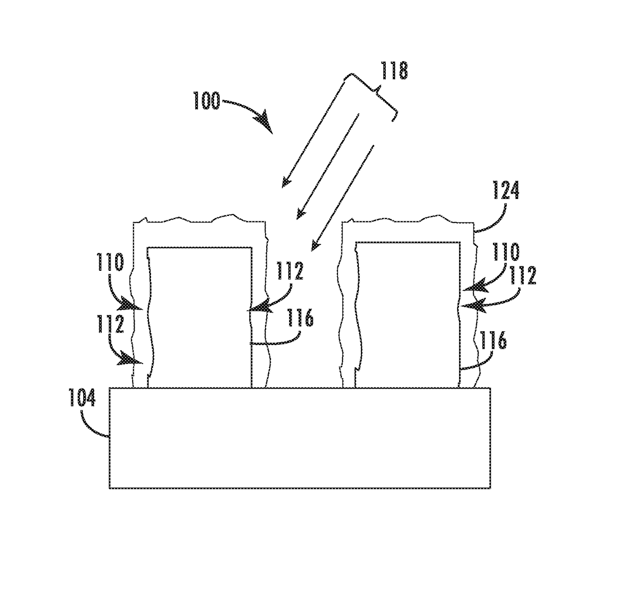
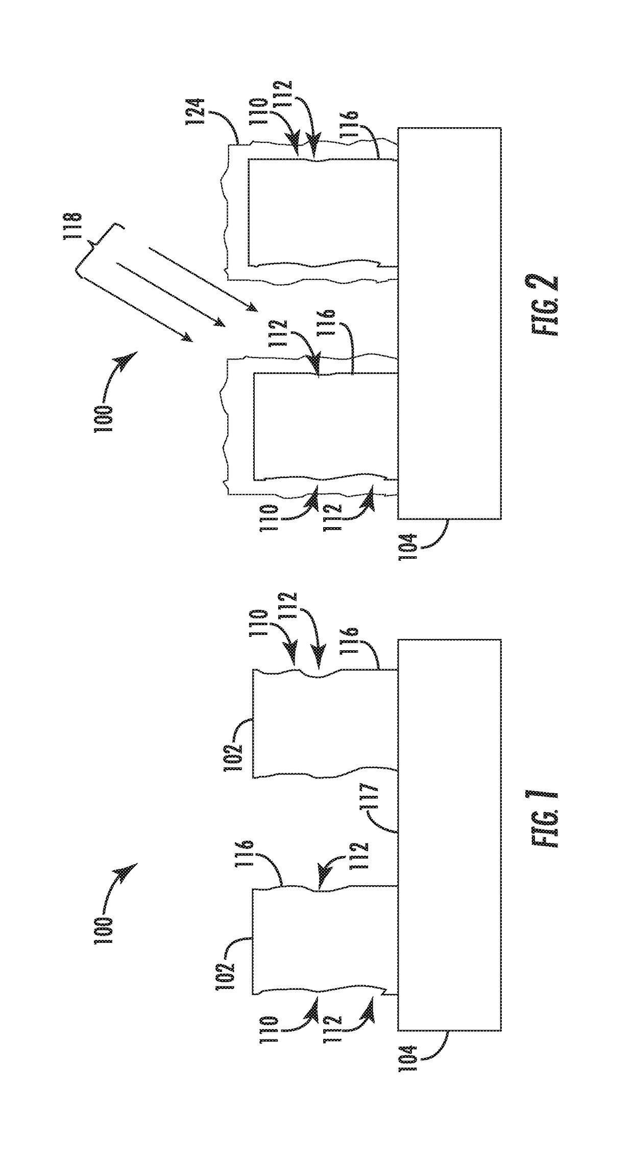
[0043]In various embodiments, sputtering can be achieved in a number of ways. In a first embodiment, demonstrated by FIG. 4A, the second ions 130 can be implanted incident at a selected angle ‘α’ (e.g., 60°) optimized for smoothing the protrusions 110 and or the film layer 124. Utilizing the inherent smoothing of angled ion implantation, combined with the preferential sputtering of high regions of deposition, LER may be reduced.
second embodiment
[0044]In a second embodiment, demonstrated by FIG. 4B, the second ions 130 may be implanted at an angle substantially parallel to a plane defined by a height ‘H’ of the patterning feature 102. In this case, the ions primarily sputter deposition fragments of the film layer 124 and portions 138 of the protrusions 110 extending outwardly, with some of the sputtered material falling into adjacent indentations 112, further smoothing the PR line.
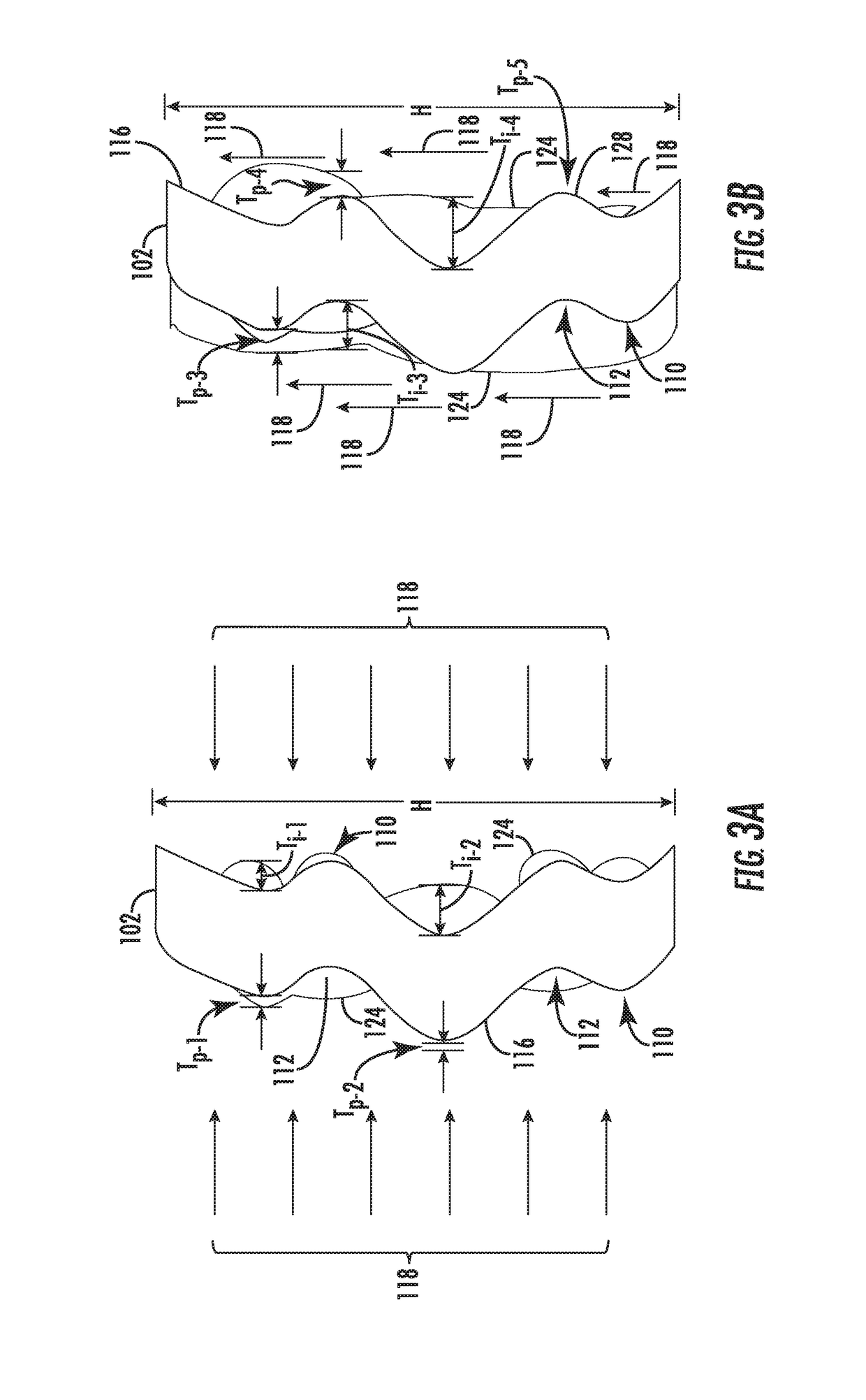
[0045]The net transformation resulting from these processes, e.g., directional film deposition and subsequent energetic ion sputter, is demonstrated by FIGS. 5A-B. In this embodiment, a mixture of CH3F and O2 is used to deposit a polymer based film layer 124 on the set of photoresist patterning features 102, as depicted in the top view and side cross sectional view (inset) depicted in FIG. 5A. Gas flow, gas ratio, implantation energy, and RF power are optimized to create a process similar to the process demonstrated in FIG. 2B, where deposition of...
PUM
| Property | Measurement | Unit |
|---|---|---|
| feature size | aaaaa | aaaaa |
| incidence angle | aaaaa | aaaaa |
| incidence angle | aaaaa | aaaaa |
Abstract
Description
Claims
Application Information