

Chemically amplified negative resist composition and patterning process
a negative resist and composition technology, applied in the field of chemical amplifying negative resist compositions, can solve the problems of rough line edges, increased seriousness, and inability to overcome the problems of conventional resist compositions, and achieve the effect of improving ler and minimizing substrate poisoning
- Summary
- Abstract
- Description
- Claims
- Application Information
AI Technical Summary
Benefits of technology
Problems solved by technology
Method used
Image

Examples
synthesis example 1
Monomer Synthesis Example 1
Preparation of triphenylsulfonium 2,2-difluoro-3-methacryloyloxypentanoate
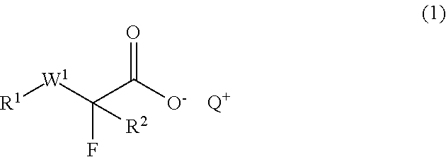
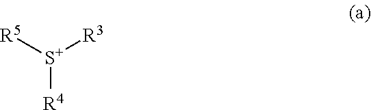
[0157]A 1-L glass flask equipped with a dropping funnel was charged with 108 g (0.486 mol) of 1-hydroxycarbonyl-1,1-difluoro-2-butyl methacrylate and 108 g of chloroform, which were stirred and cooled at 0° C. Then 224 g (0.560 mol / 1.15 equivalent) of a 10 wt % sodium hydroxide aqueous solution was added dropwise to the solution, which was stirred at room temperature for 1 hour. Then 169 g (0.492 mol / 1.01 equivalent) of triphenylsulfonium bromide in 432 g of chloroform was added to the solution, which was stirred at room temperature for 1 hour. After the completion of reaction was confirmed by 1H-NMR spectroscopy, an organic layer was separated from the reaction liquid and washed 3 times with 300 g of water. The organic layer was concentrated in vacuum, obtaining 238 g (yield 81%, purity 80%) of triphenylsulfonium 2,2-difluoro-3-methacryloyloxy-pentanoate, designated Monomer Z-1, hav...
polymer synthesis example 1
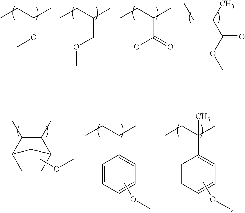
[0161]In a 200-mL dropping funnel under nitrogen blanket, a solution was prepared by dissolving 33.2 g of 4-hydroquinone monomethacrylate, 4.7 g of acenaphthylene, 10.6 g of 4-methylstyrene, 1.5 g of Monomer Z-1, and 5.7 g of dimethyl 2,2′-azobis(2-methylpropionate) (V601, Wako Pure Chemical Industries, Ltd.) in 70 g of methyl ethyl ketone (MEK) as a solvent. A 300-mL polymerization flask was purged with nitrogen, charged with 50 g of MEK, and heated at 80° C., after which the solution was added dropwise to the flask over 4 hours. After the completion of dropwise addition, stirring was continued for 16 hours to effect polymerization while maintaining the temperature of 80° C. The polymerization solution was then cooled down to room temperature and added dropwise to 1,000 g of hexane for precipitation. The copolymer precipitate was collected by filtration and washed twice with 200 g of hexane. The mass collected by filtration was dissolved in 120 g of MEK. The MEK solution was passed...
polymer synthesis example 2
[0162]In a 500-mL dropping funnel under nitrogen blanket, a solution was prepared by dissolving 76.0 g of 4-(1-ethoxyethoxy)styrene, 8.6 g of acenaphthylene, 12.7 g of 4-methylstyrene, 2.7 g of Monomer Z-1, and 10.4 g of dimethyl 2,2′-azobis(2-methylpropionate) (V601, Wako Pure Chemical Industries, Ltd.) in 112 g of propylene glycol monomethyl ether (PGME) as a solvent. A 500-mL polymerization flask was purged with nitrogen, charged with 75 g of PGME, and heated at 80° C., after which the solution was added dropwise to the flask over 4 hours. After the completion of dropwise addition, stirring was continued for 20 hours to effect polymerization while maintaining the temperature of 80° C. The polymerization solution was then cooled down to room temperature. To the solution were added 25 g of methanol and 1.25 g of oxalic acid dihydrate. The mixture was stirred for 3 hours at 50° C. The reaction solution was added dropwise to a mixture of 2,000 g of water and 50 g of methanol for prec...
PUM
| Property | Measurement | Unit |
|---|---|---|
| size | aaaaa | aaaaa |
| wavelength | aaaaa | aaaaa |
| size | aaaaa | aaaaa |
Abstract
Description
Claims
Application Information