Eureka AIR delivers breakthrough ideas for toughest innovation challenges, trusted by R&D personnel around the world.

Display device including sensor screen

a display device and sensor technology, applied in printing image acquisition, instruments, computing, etc., can solve the problems of increased size, increased product cost, increased size, etc., and achieve the effect of increasing the fingerprint recognition rate and the rigidity of the display panel when the two transparent substrates are disposed on the display panel

Active Publication Date: 2017-11-30
LG DISPLAY CO LTD
View PDF11 Cites 18 Cited by
  • Summary
  • Abstract
  • Description
  • Claims
  • Application Information

AI Technical Summary

Benefits of technology

This patent describes a display device with a sensor screen that has increased rigidity when two transparent substrates are used compared to one substrate, which leads to better protection from external impact. The fingerprint sensor is placed between the substrates, leading to better fingerprint recognition. Additionally, the device can perform touch recognition and fingerprint sensing simultaneously. The fingerprint sensor is placed in the display area, allowing for precise sensing regardless of the environment.

Problems solved by technology

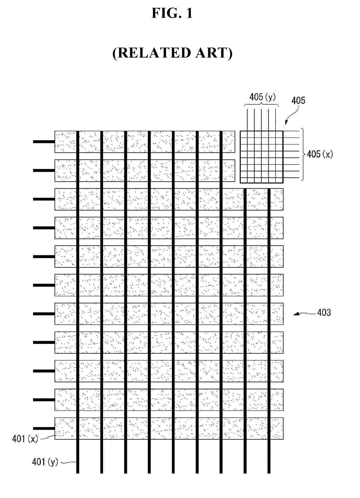
However, problems in this field concern an increase in size due to the use of LEDs and a rise in the product cost due to the use of expensive light source.
However, when the IC and the high resolution sensor array are integrated using the silicon wafer, the small-sized packaged fingerprint sensor has to be embedded in a push button (e.g., a home key of a smart phone) or separately attached to a back surface of the push button because the silicon wafer is opaque and has a limit to an increase in size.
Thus, an assembly configuration for coupling the fingerprint sensor with the push button is necessary, thereby leading to an increase in size (due to a non-display area and a thickness) and a rise in the product cost.
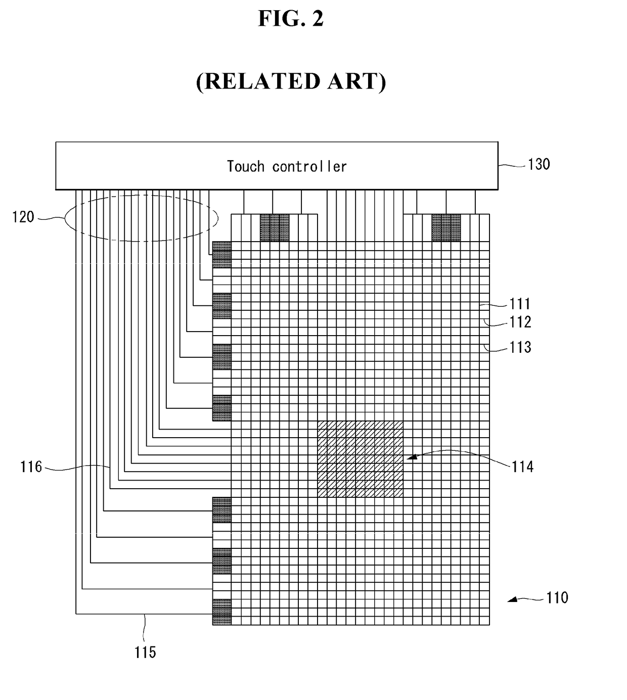
Because an increase in the mutual capacitance reduces sensitivity of the touch sensor, a touch operation may not be recognized when the touch operation is generated.

Method used


Image

  • Display device including sensor screen
  • Display device including sensor screen
  • Display device including sensor screen

Examples


Embodiment Construction

[0059]Reference will now be made in detail to embodiments of the invention, examples of which are illustrated in the accompanying drawings. Wherever possible, the same reference numbers will be used throughout the drawings to refer to the same or like parts. Detailed description of known arts will be omitted if it is determined that the arts can mislead the embodiments of the invention. Names of the respective elements used in the following explanations are selected only for convenience of writing the specification and may be thus different from those used in actual products.

[0060]In the following description, “first display area” is a main display part of a display device and means “a main display area” capable of sensing a touch; “second display area” is an auxiliary display part, in which a selection icon, etc. are displayed, and means “a sub-display area” capable of sensing a fingerprint input and a touch input; and “fingerprint touch area” means an area that is positioned in th...


PUM


Abstract

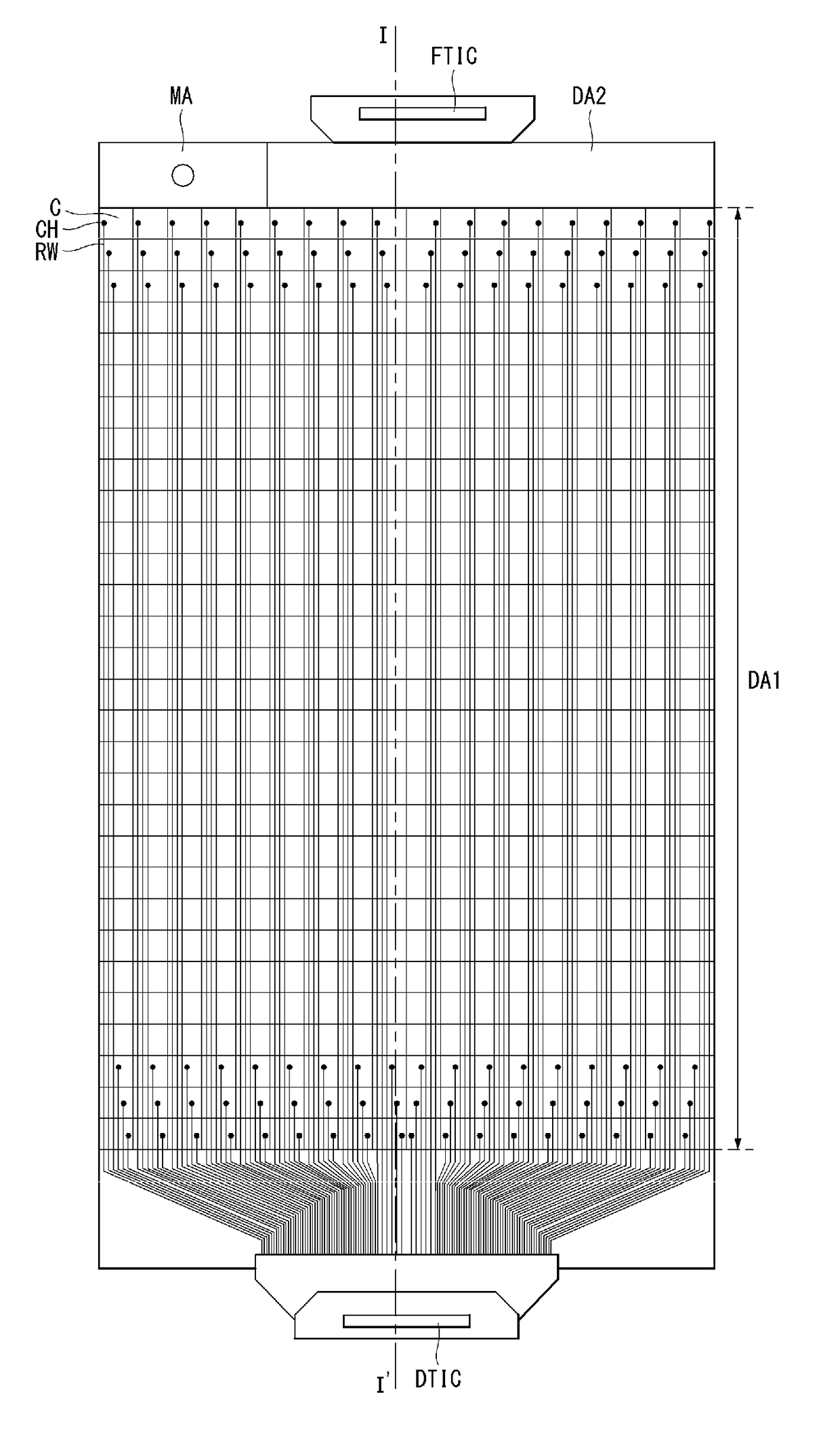
A display device including a sensor screen having a touch recognition function and a fingerprint recognition function is disclosed. The display device includes a display panel having a first display area and a second display area that are adjacent to each other, a first touch sensor being disposed in the first display area, and a sensor screen having a first transparent substrate and a second transparent substrate that are sequentially disposed on the display panel, and a fingerprint sensor and a second touch sensor that are disposed between the first transparent substrate and the second transparent of the sensor screen corresponding to the second display area of the display panel.

Description

[0001]This application claims the benefit of priority under 35 U.S.C. §119(a) to Republic of Korean Patent Application No. 10-2016-0066555 filed on May 30, 2016, the entire contents of which is incorporated herein by reference for all purposes as if fully set forth herein.BACKGROUNDField of the Invention[0002]The present disclosure relates to a display device including a sensor screen, and more particularly, to a display device including a sensor screen having a touch recognition function and a fingerprint recognition function.Discussion of the Related Art[0003]With the development of computer technology, computer based systems, that can be applied to various utilities such as notebook computers, tablet personal computers (PCs), smart phones, personal digital assistants (PDAs), automated teller machines (ATMs), and information systems, have been developed. In general, computer based systems store various data including private information such as secret business information and pers...

Claims


Application Information

Patent Timeline
IPC IPC(8): G06F3/044G06K9/00G06F3/041
CPCG06F3/044G06F3/0416G06K9/0002G06F3/0412G06V40/1306G06F2203/0338G06F2203/04103G06F3/04886G06F3/04166G06F3/0446G06F3/0443G06V40/13G06F3/0445G06F3/0448G06F2203/04106G06F2203/04111
Inventor HAN, MANHYEOPCHOO, KYOSEOPLEE, BUYEOLSONG, MOONBONGCHO, JIHO
Owner LG DISPLAY CO LTD
Why Eureka
Eureka Blog
Learn More