Touch sensor and touch panel

Inactive Publication Date: 2017-12-28
FUJIFILM CORP
View PDF9 Cites 14 Cited by
  • Summary
  • Abstract
  • Description
  • Claims
  • Application Information

AI Technical Summary

Benefits of technology

[0017]According to the touch sensor of the present invention and the touch panel in which the touch sensor is used, it is possible to reduce the size by simplifying the constitution and

Problems solved by technology

Since the mobile terminal device has a structure in which an antenna module is separately prepared and a built-in substrate and the antenna module are connected with each other using a cable, it is not always true that the optimal antenna module installation space can be secured.
In addition, the antenna module has a structure that becomes complicated depending on limited spaces, and thus it is difficult to reduce the costs.
Meanwhile, as means for equipping the built-in substrate with antenna functions, there is a method in which a small-size chip antenna to

Method used


Image

  • Touch sensor and touch panel
  • Touch sensor and touch panel
  • Touch sensor and touch panel

Examples


Example

[0045]Next, a touch panel of a first embodiment of the present invention will be described.

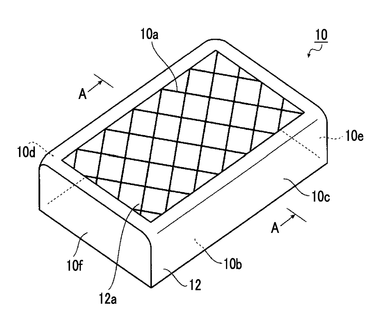
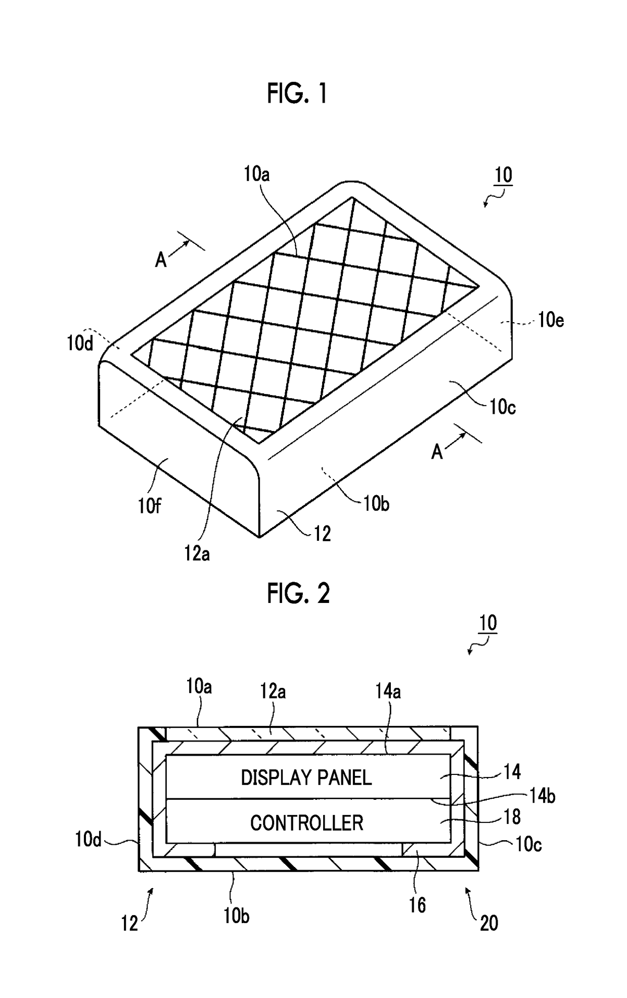
[0046]FIG. 1 is a perspective view illustrating an electronic device including the touch panel of the first embodiment of the present invention, and FIG. 2 is a cross-sectional view in a direction of A-A line in FIG. 1.

[0047]An electronic device 10 illustrated in FIG. 1 and FIG. 2 has a three-dimensional shape and has a touch panel 20 of an embodiment of the present invention therein.

[0048]The electronic device 10 includes a chassis 12 having a three-dimensional shape which constitutes the outer form, and a display panel 14, a touch sensor 16, and a controller 18 are provided in the chassis 12. The touch sensor 16 is disposed on a display surface 14a of the display panel 14. While described in detail below, the touch sensor 16 has a three-dimensional shape. The controller 18 is provided on a rear surface 14b of the display panel 14. A touch panel 20 having a three-dimensional shape is constitu...

Example

[0117]Next, a touch panel of a second embodiment of the present invention will be described.

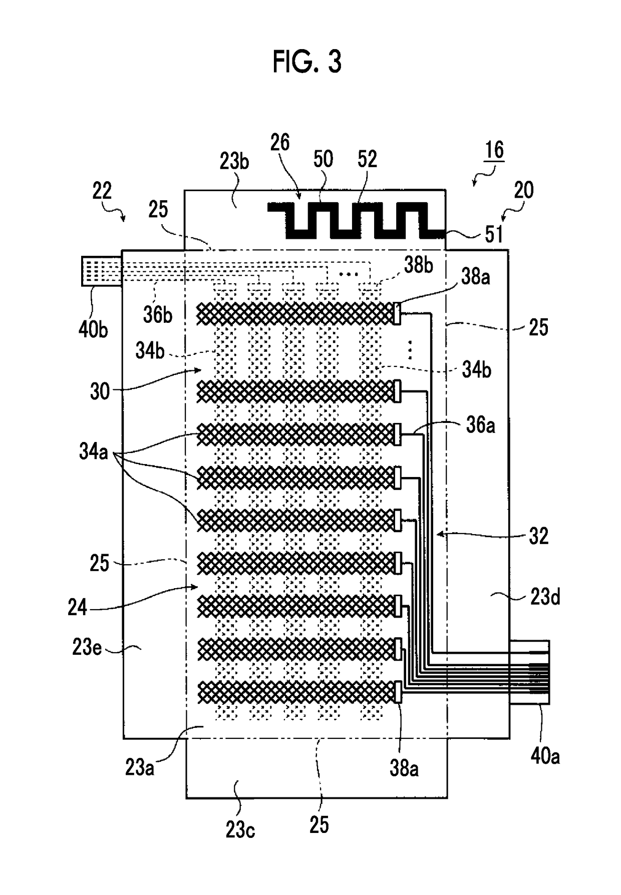
[0118]FIG. 11 is a schematic plan view illustrating the touch panel of the second embodiment of the present invention. FIG. 12 is a schematic cross-sectional view illustrating an electronic device including the touch panel of the second embodiment of the present invention. FIG. 13 is a schematic view illustrating an example of an antenna.

[0119]Meanwhile, in a touch panel 60, a touch sensor 16a, and an electronic device 11 in the present embodiment illustrated in FIGS. 11 to 13, the same components as those in the touch panel 20, the touch sensor 16, and the electronic device 10 in the first embodiment will be given the same reference sign and will not be described in detail.

[0120]Compared with the touch panel 20 (refer to FIG. 3) and the touch sensor 16 (refer to FIG. 3) of the first embodiment, the touch panel 60 and the touch sensor 16a in the present embodiment, which are illustrated in FI...

Example

[0135]Next, a touch panel of a third embodiment of the present invention will be described.

[0136]FIG. 14 is a schematic plan view illustrating the touch panel of the third embodiment of the present invention.

[0137]Meanwhile, in a touch panel 80 and a touch sensor 82 in the present embodiment illustrated in FIG. 14, the same components as those in the touch panel 20, the touch sensor 16, and the electronic device 10 in the first embodiment will be given the same reference sign and will not be described in detail.

[0138]Compared with the touch panel 20 (refer to FIG. 3) of the first embodiment and the touch sensor 16 (refer to FIG. 3), the touch panel 80 and the touch sensor 82 in the present embodiment, which are illustrated in FIG. 14, have a difference in terms of the independent provision of touch sensor portions 24a in the side surface regions 23c, 23d, and 23e of the substrate 22, and other constitutions are the same as the constitutions of the touch panel 20, the touch sensor 16...


PUM


Abstract

A touch sensor has one substrate having a plurality of regions that are at least a planar region and a side surface region which is continuous to the planar region and is bent with respect to the planar region, a touch sensor portion provided in the planar region of the substrate, and an antenna provided in a region other than the planar region of the substrate. The substrate is constituted of a flexible transparent substrate. The touch sensor portion includes a detection portion and a peripheral wire portion, and at least the detection portion is constituted of a thin metal wire.

Description

CROSS-REFERENCE TO RELATED APPLICATIONS[0001]This application is a Continuation of PCT International Application No. PCT / JP2016 / 055084 filed on Feb. 22, 2016, which claims priority under 35 U.S.C. §119(a) to Japanese Patent Application No. 2015-067252 filed on Mar. 27, 2015. The above application is hereby expressly incorporated by reference, in its entirety, into the present application.BACKGROUND OF THE INVENTION1. Field of the Invention[0002]The present invention relates to a touch sensor that can be used together with display devices such as liquid crystal display devices and a touch panel in which the touch sensor is used and particularly to a touch sensor including an antenna and a touch panel in which the touch sensor including an antenna is used.2. Description of the Related Art[0003]At the moment, for mobile terminal devices equipped with touch panels which are called smartphones, tablets, or the like, efforts are being made to improve the functions and reduce the size, thi...

Claims


Application Information

Patent Timeline
IPC IPC(8): G06F3/044H01Q1/52H01Q1/24
CPCG06F3/044H01Q1/526G06F2203/04107G06F2203/04112H01Q1/24G06F3/04164G06F3/0445G06F3/0446H01Q1/243H01Q9/42G06F2203/04111
Inventor ENDO, YASUSHITADA, NOBUYUKI
Owner FUJIFILM CORP
Why Eureka
Try Eureka