
Eureka
For R&D, Eureka makes reading and utilizing patents & technical documents easy.
Eureka AIR
Designed for self-driven R&D workflows. Generate viable solutions, solve complex R&D challenges, empower your innovation with AI.

Eureka Materials
Designed for material experts only. Revolutionize your material R&D, from search, analyze, to developing new materials.

TechResearch
Generate reliable direction feasibility study reports for your R&D in just a few steps.

TechSeek
Discover and master advanced knowledge NOW. Basics, ideas, possibilities, all at once.

TechMind
As an expert in R&D Theories, TechMind can generates customized viable solutions instantly.

TechRisk
Analyze your overall solution with one click, know your potential R&D risks in advance.

TechMonitor
Get weekly tech updates, stay abreast of the latest tech innovations and key insights.
Memory auto repairing circuit and associated method
- Summary
- Abstract
- Description
- Claims
- Application Information
AI Technical Summary
Benefits of technology
Problems solved by technology
Method used
Image

Examples
first embodiment
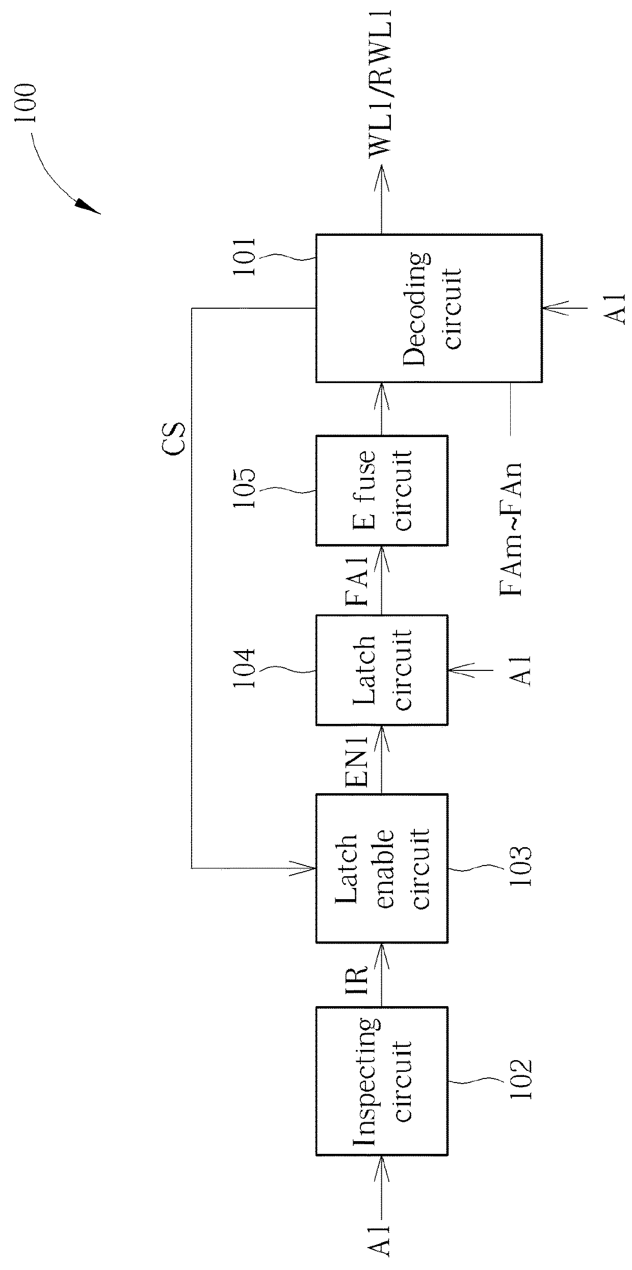
[0012]FIG. 1 is a diagram illustrating a memory auto repairing circuit 100 according to the present invention. As shown in FIG. 1, the memory auto repairing circuit 100 comprises a decoding circuit 101, an inspecting circuit 102, a latch enable circuit 103, a latch circuit 104, and an E-fuse circuit 105. The decoding circuit 101 is arranged to receive an input address, e.g. an address A1 shown in FIG. 1, and decode the address A1 to determine if the address A1 corresponds to one of fail addresses FAm-FAn. If the address A1 corresponds to one of the fail addresses FAm-FAn, a redundancy word line previously allocated to the fail address will be accessed. It should be noted that the fail addresses FAm-FAn are usually stored in a plurality of E-fuse circuits. For clarity and simplicity, only the E-fuse circuit 104 relevant to this embodiment is depicted in FIG. 1. The decoding circuit 101 is further arranged to generate a control signal CS when the address A1 corresponds to one of the f...
second embodiment
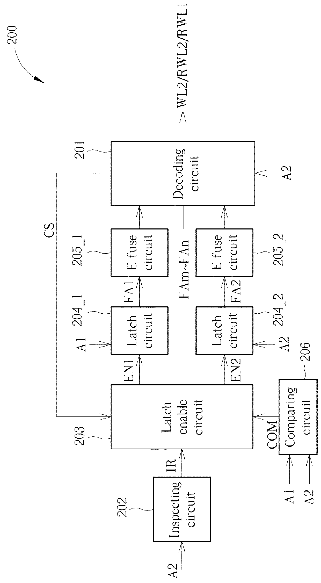
[0014]FIG. 2 is a diagram illustrating a memory auto repairing circuit 200 according to the present invention. The memory auto repairing circuit 200 comprises a decoding circuit 201, an inspecting circuit 202, a latch enable circuit 203, latch circuits 204_1 and 204_2, E-fuse circuits 205_1 and 205_2, and a comparing circuit 206. In this embodiment, the address A1 has been stored into the latch circuit 204_1 according to the enable signal EN1 as in the embodiment of FIG. 1. The decoding circuit 201 is arranged to receive an input address, e.g. an address A2 shown in FIG. 2, and decode the address A2 to determine if the address A2 corresponds to one of the fail addresses FAm-FAn. If the address A2 corresponds to one of the fail addresses FAm-FAn, the redundancy word line previously allocated to the fail address is accessed. As mentioned in the embodiment of FIG. 1, the decoding circuit 201 is further arranged to generate the control signal CS when the address A2 corresponds to any of...
third embodiment
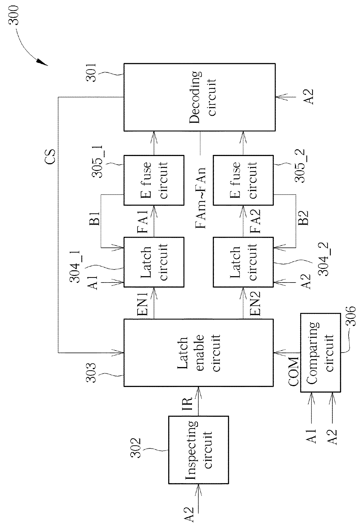
[0016]FIG. 3 is a diagram illustrating a memory auto repairing circuit 300 according to the present invention. The memory auto repairing circuit 300 comprises a decoding circuit 301, an inspecting circuit 302, a latch enable circuit 303, latch circuits 304_1 and 304_2, E-fuse circuits 305_1 and 305_2, and a comparing circuit 306, wherein the functions of the decoding circuit 301, the inspecting circuit 302, the latch enable circuit 303, the latch circuits 304_1 and 304_2, the E-fuse circuits 305_1 and 305_2, and the comparing circuit 306 are similar / identical to those described in the embodiment of FIG. 2. The only difference is the E-fuse circuit 305_1 is further arranged to generate a burned signal B1 to the latch circuits 304_1 when the address A1 is stored into the E-fuse circuit 305_1 as the fail address FA1. Once the burned signal B11 is received by the latch circuit 304_1, the latch circuit 304_1 will no longer store any input address. Likewise, the E-fuse circuit 305_2 is fu...
PUM
 Abstract
Description
Claims
Application Information
 - R&D Engineer
- R&D Manager
- IP Professional
- Industry Leading Data Capabilities
- Powerful AI technology
- Patent DNA Extraction
Browse by: Latest US Patents, China's latest patents, Technical Efficacy Thesaurus, Application Domain, Technology Topic, Popular Technical Reports.
© 2024 PatSnap. All rights reserved.Legal|Privacy policy|Modern Slavery Act Transparency Statement|Sitemap|About US| Contact US: help@patsnap.com