Method of controlling display of operation of semiconductor manufacturing apparatus and non-transitory computer readable storage medium therefor, and system for performing display concerning operation of semiconductor manufacturing apparatus

a semiconductor manufacturing apparatus and display technology, applied in the field of display concerning the operation of the semiconductor manufacturing apparatus, can solve the problems of significant time and effort, inability to make the development of an abnormality easily understandable, and the character and numerical value of the history data which includes characters and numerical values is not easily understood by people, so as to achieve the effect of making the development of a certain condition in the semiconductor manufacturing apparatus easy to understand

Active Publication Date: 2018-10-04
EBARA CORP
View PDF6 Cites 4 Cited by
  • Summary
  • Abstract
  • Description
  • Claims
  • Application Information

AI Technical Summary

Benefits of technology

[0017]According to an embodiment of the present invention, such an animation as to make development of

Problems solved by technology

The history data which includes characters and numerical values are not easily understandable by people.
To analyze the data, significan

Method used


Image

  • Method of controlling display of operation of semiconductor manufacturing apparatus and non-transitory computer readable storage medium therefor, and system for performing display concerning operation of semiconductor manufacturing apparatus
  • Method of controlling display of operation of semiconductor manufacturing apparatus and non-transitory computer readable storage medium therefor, and system for performing display concerning operation of semiconductor manufacturing apparatus
  • Method of controlling display of operation of semiconductor manufacturing apparatus and non-transitory computer readable storage medium therefor, and system for performing display concerning operation of semiconductor manufacturing apparatus

Examples


Embodiment Construction

[0038]Hereinafter, an embodiment of the present invention is described in detail with reference to the drawings. The following description is merely an example according to the embodiment of the present invention. Accordingly, the present invention is not limited to the following description, and various modifications can be made within the scope without departing from the gist of the invention.

1 the Structure of a System According to an Embodiment of the Present Invention

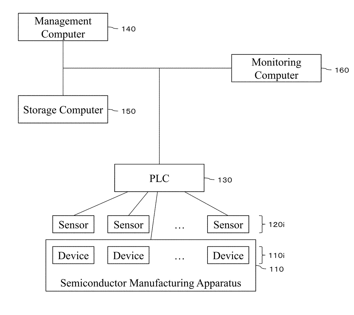
[0039]FIG. 1 illustrates the configuration of a system according to an embodiment of the present invention. The blocks in FIG. 1 represent components of the system. In FIG. 1, straight lines connecting the components to each other represent main transmission routes for information (including signals and data, etc.) among the components. At least one of two components connected with each other by one of the straight lines can transmit information to the other component. At least one of two components connected with ...


PUM


Abstract

A method is provided, the method including: repeatedly acquiring a state of one or more devices included in the semiconductor manufacturing apparatus; providing a first animation indicating an operation of the semiconductor manufacturing apparatus by displaying at least an image indicating the state of one or more devices on a display unit each time the state is acquired; storing, in a memory, the acquired state of one or more devices and a time related to the state; receiving an input for switching a display mode; and providing a second animation of the semiconductor manufacturing apparatus by displaying, one by one on the display unit, at least one or more images respectively indicating the state of one or more devices related to one or more times including a reference time stored in the memory, after receiving the input for switching a display mode.

Description

TECHNICAL FIELD[0001]The present invention relates to a display concerning an operation of a semiconductor manufacturing apparatus.BACKGROUND ART[0002]In a semiconductor manufacturing apparatus, the states of semiconductor devices including the state of a semiconductor substrate which is being manufactured are monitored. The history of alarms corresponding to abnormalities, etc. in the states and the history of semiconductor manufacturing processes, etc. are displayed on a computer that is directly or indirectly connected to the apparatus. When a trouble has occurred in the semiconductor manufacturing apparatus, past operations of the semiconductor manufacturing apparatus are estimated on the basis of the history data displayed on the computer or the like. The history data which includes characters and numerical values are not easily understandable by people. To analyze the data, significant time and effort are required.[0003]In this regard, for example, Japanese Patent Laid-Open No...

Claims


Application Information

Patent Timeline
IPC IPC(8): H01L21/67G06F3/0484G06F3/147C25D17/00
CPCH01L21/67276G06F3/04847G06F3/147C25D17/001G06T13/80G06T2200/24G05B19/4183G05B2219/31282C25D17/00C25D21/12G05B19/418G05B23/027G05B23/0272G05B2219/23129G05B2219/23171G05B2219/24072G05B19/46Y02P90/02
Inventor FUJIKI, MASAYUKIAOYAMA, HIDEHARUKOIZUMI, RYUYA
Owner EBARA CORP
Why Eureka
Try Eureka