Touch panel and fabrication method thereof
a technology of touch panel and fabrication method, which is applied in the field of touch panel, can solve the problems of high manufacturing cost, limited manufacturing process and design of touch display devices, and limited black border layer through holes
- Summary
- Abstract
- Description
- Claims
- Application Information
AI Technical Summary
Benefits of technology
Problems solved by technology
Method used
Image

Examples
Embodiment Construction
[0034]Reference will now be made in detail to the present embodiments of the invention, examples of which are illustrated in the accompanying drawings. Wherever possible, the same reference numbers are used in the drawings and the description to refer to the same or like parts.
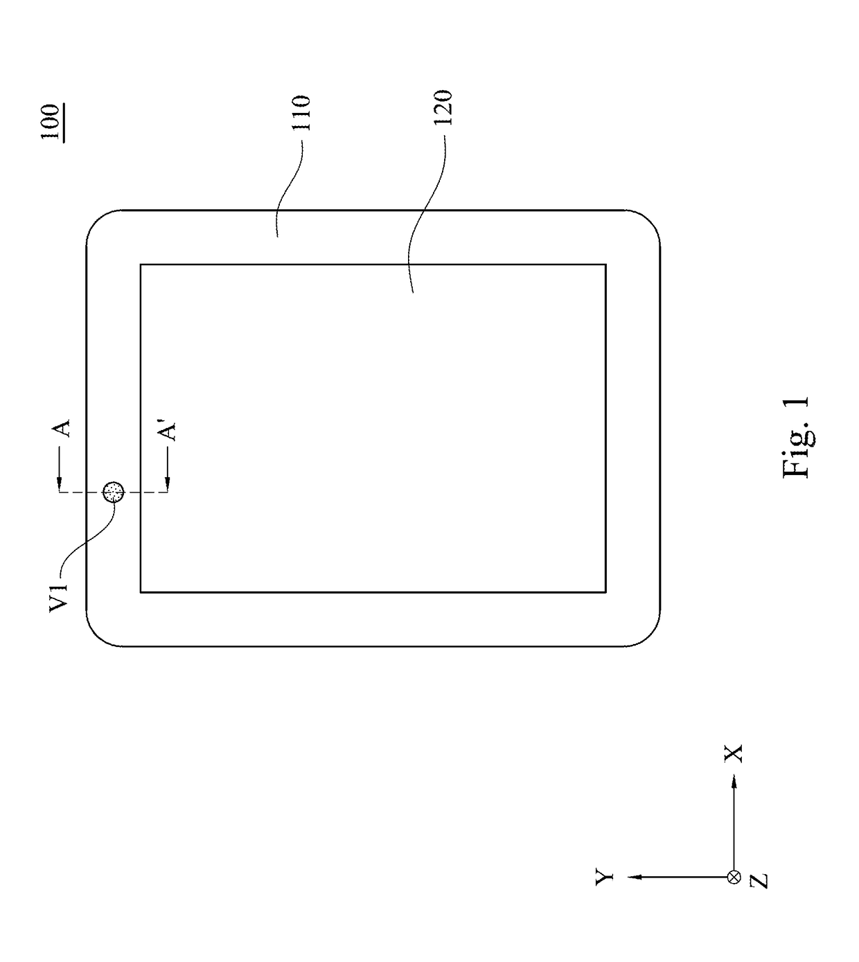
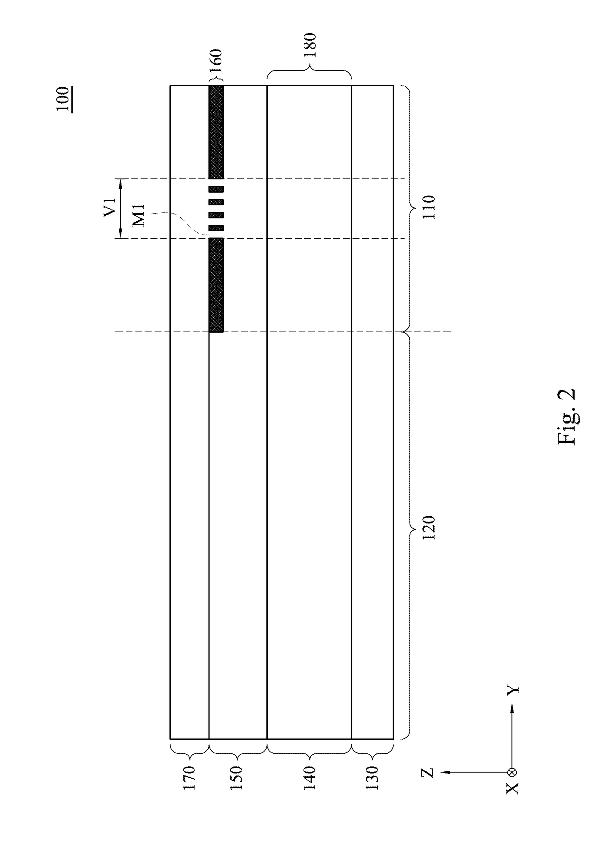
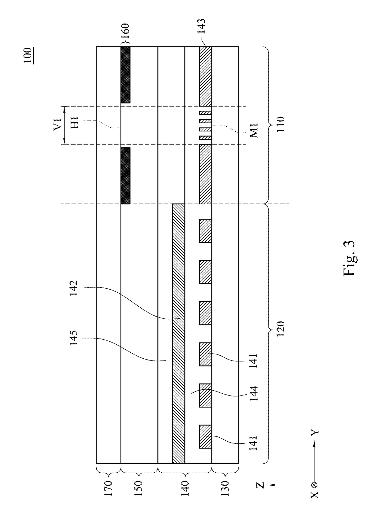
[0035]FIG. 1 is a top view of a touch panel according to an embodiment of the present invention. FIG. 2 is a cross-sectional view illustrating a conventional touch panel with an ambient light sensing region V1, taken along the line A-A′ of FIG. 1. As shown in FIG. 1 and FIG. 2, a touch panel 100 has an ambient light sensing region V1. The touch panel 100 includes a transparent substrate 130, a touch-sensing electrode layer 140, a cured optical adhesive layer 150, a light transparent material layer 180, and a cover glass 170. The transparent substrate 130 has a touch-sensing region 120 and a peripheral region 110. The touch-sensing electrode layer 140 is disposed on the touch-sensing region 120 of the transpare...
PUM
 Abstract
Description
Claims
Application Information