Display device

a technology of a display device and a display screen, which is applied in the direction of semiconductor devices, basic electric elements, electrical equipment, etc., can solve the problems of non-uniform image quality, and achieve the effect of improving the reliability of thin film encapsulation and uniform image quality

Active Publication Date: 2019-05-16
SAMSUNG DISPLAY CO LTD
View PDF2 Cites 19 Cited by
  • Summary
  • Abstract
  • Description
  • Claims
  • Application Information

AI Technical Summary

Benefits of technology

[0006]Exemplary embodiments of the invention provide a display device that displays an image having uniform image quality and is improved in thin film encapsulation reliability.

Problems solved by technology

As the resistance increases, a voltage level may vary according to a position, thereby causing non-uniform image quality.

Method used


Image

  • Display device
  • Display device
  • Display device

Examples


Embodiment Construction

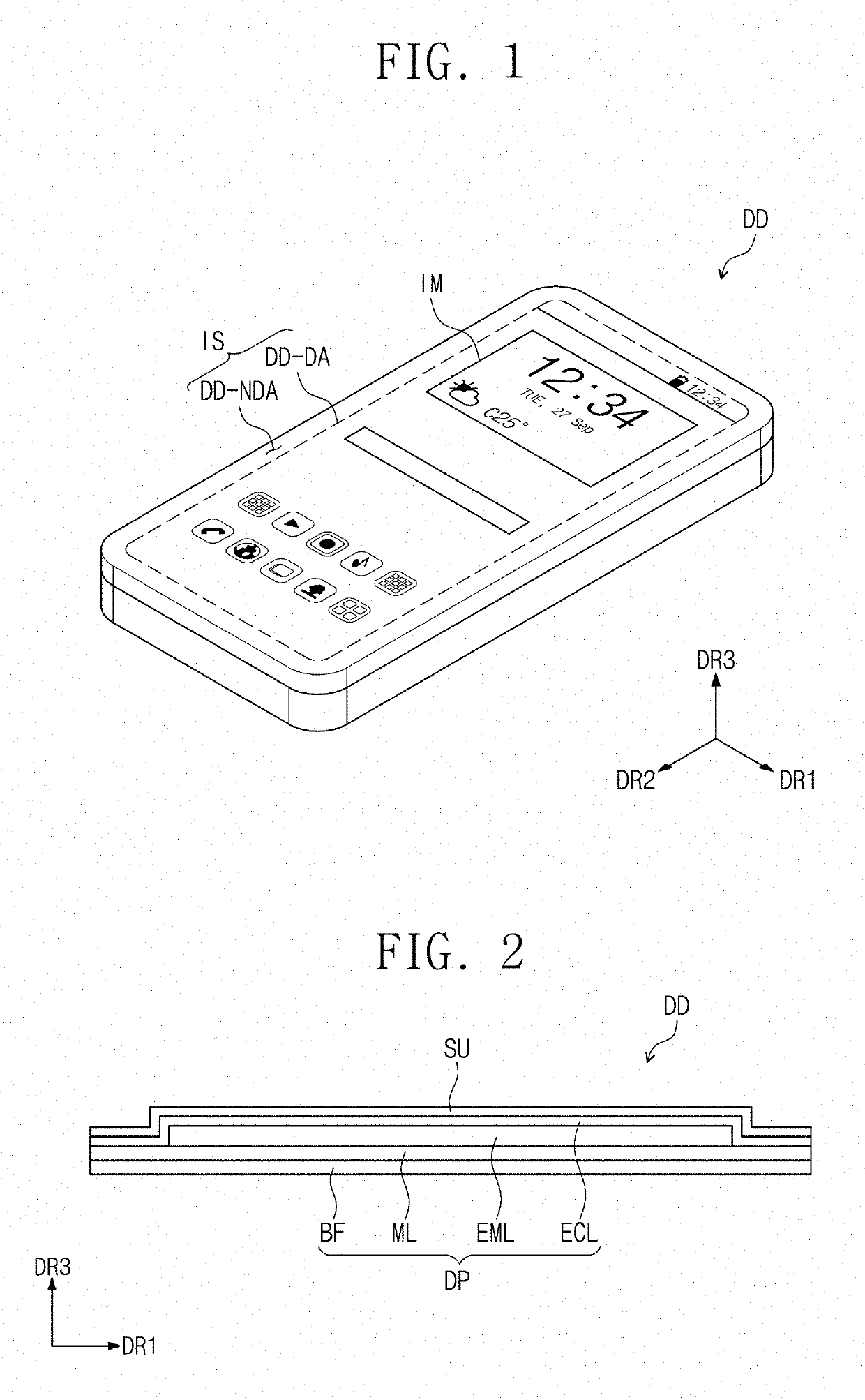
[0050]Hereinafter, exemplary embodiments of the invention will be described with reference to the accompanying drawings. In this specification, it will also be understood that when one component (or region, layer, portion, etc.) is referred to as being ‘on’, ‘connected to’, or ‘coupled to’ another component, it can be directly connected / coupled on / to the one component, or an intervening third component may also be present.

[0051]Like reference numerals refer to like elements throughout. Also, in the drawing figures, the thickness, ratio, and dimensions of components are exaggerated for clarity of illustration. The term “and / or” includes any and all combinations of one or more of the associated listed items.

[0052]It will be understood that although the terms such as ‘first’ and ‘second’ are used herein to describe various elements, these elements should not be limited by these terms. The terms are only used to distinguish one component from other components. For example, a first eleme...


PUM


Abstract

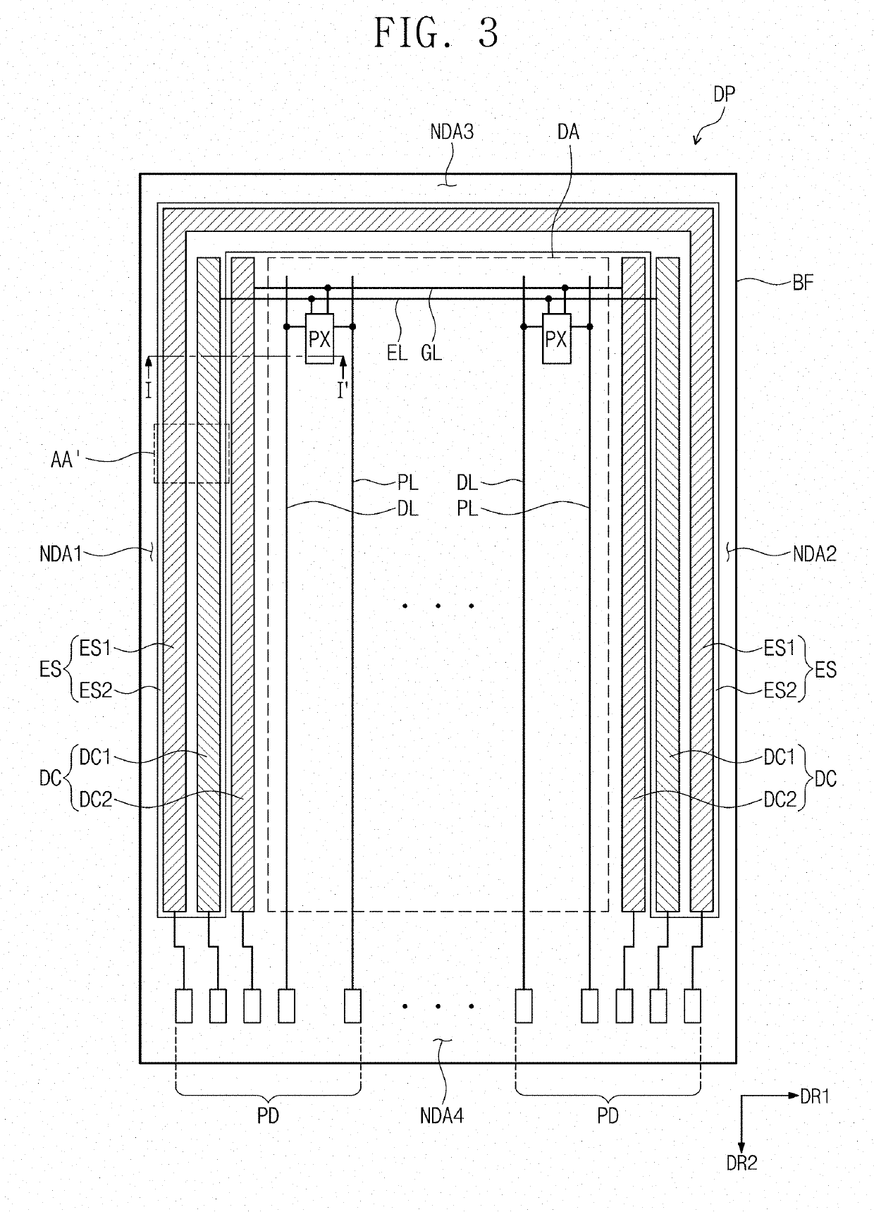
A display device includes a base layer on which a display area and a non-display area are defined, a circuit layer including a first power electrode and driving circuits, which are disposed in the non-display area, a first planarization layer in which a first opening through which the first power electrode is exposed is defined and which covers the driving circuits, a second power electrode disposed on the first planarization layer to contact the first power electrode that is exposed through the first opening and overlapping at least a portion of the driving circuits, and a second planarization layer disposed on the first planarization layer to cover a portion of the second power electrode and having a groove part in an area overlapping the first planarization layer and the second power electrode in a plan view.

Description

[0001]This application claims priority to Korean Patent Application No. 10-2017-0153374, filed on Nov. 16, 2017, and all the benefits accruing therefrom under 35 U.S.C. § 119, the content of which in its entirety is herein incorporated by reference.BACKGROUND1. Field[0002]Exemplary embodiments of the invention herein relate to a display device that is improved in image quality and thin film encapsulation reliability.2. Description of Related Art[0003]A display device may be divided into a display area on which an image is display and a non-display area disposed around the display area. Recently, various studies have been made to reduce a width of the non-display area to increase the display area on which an image is displayed. However, as the non-display area is reduced, an area of elements integrated in the non-display area may be reduced in surface area, and thus, resistance increases. As the resistance increases, a voltage level may vary according to a position, thereby causing n...

Claims


Application Information

Patent Timeline
Patent Type & Authority Applications(United States)
IPC IPC(8): H01L27/32H01L51/52
CPCH01L27/3246H01L51/5253H01L27/3258H10K59/124H10K59/1315H10K59/131H10K50/82H10K59/122H10K50/805H10K50/84H10K50/844
Inventor LHEE, ZAILLEE, KEUNSOO
Owner SAMSUNG DISPLAY CO LTD
Why Eureka
Try Eureka