Module and electronic device

a technology of electronic devices and modules, applied in the field of modules and electronic devices, can solve the problems of deteriorating communication quality, reducing communication quality, and complicated structure of communication devices

Active Publication Date: 2019-06-13
FANUC LTD
View PDF4 Cites 0 Cited by
  • Summary
  • Abstract
  • Description
  • Claims
  • Application Information

AI Technical Summary

Benefits of technology

[0025]The present invention enables to provide a module and an electronic device each hardly deteriorating in communication quality even by attachment and detachment (putting in and taking out) of a module, vibration, impact and aged deterioration, and each hardly deteriorating in communication quality because of a structure being less complicated even by increasing the number of stacked modules.

Problems solved by technology

Such an electronic device in which communication between a plurality of modules is performed via electrical contacts as described above has a problem in that attachment and detachment (putting in and taking out) of a module, vibration and impact cause contact wear, resulting in deteriorating the communication quality thereof.
The electronic device has another problem in that aged deterioration such as oxidation of the surface of a contact lowers the communication quality.
The electronic device of Patent Document I has another problem in that in the case where the electronic device is designed to have a larger number of stacked modules, the optical communication cell is required to be extended, whereby the structure thereof becomes complicated.
The module of Patent Document 2 has another problem in that the structure itself is complicated.
Accordingly, there is a problem in that the complicated structure for bending the optical path is required.

Method used


Image

  • Module and electronic device
  • Module and electronic device
  • Module and electronic device

Examples


first embodiment

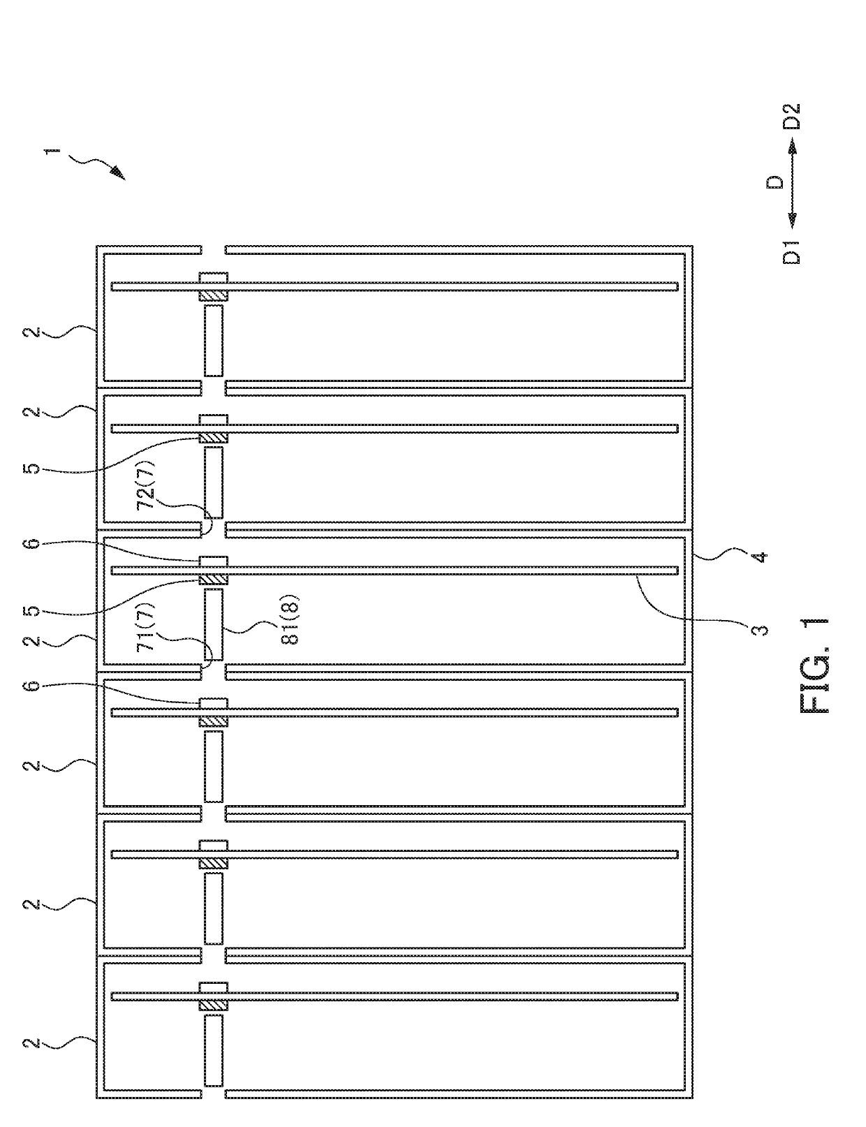
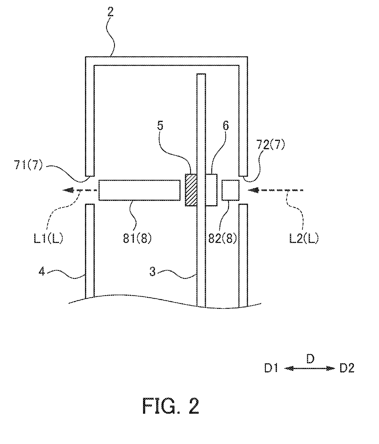
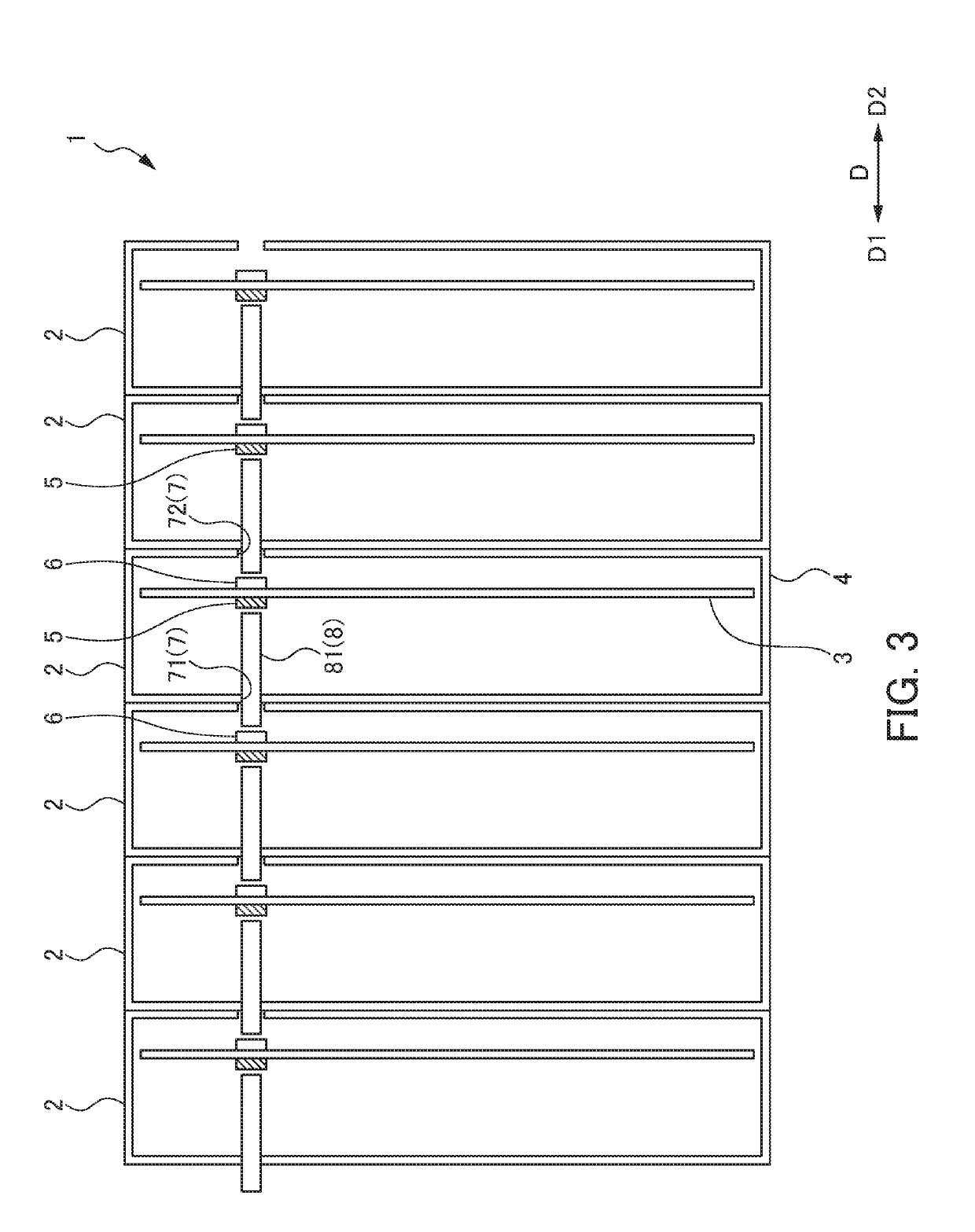
[0040]The first embodiment of the present invention is described with reference to FIG. 1 and FIG. 2. As shown in FIG. 1, an electronic device 1 is configured with a plurality of modules 2 disposed adjacent to each other, of the present embodiment. The direction in which the plurality of modules 2 are adjacent is referred to as “adjacent direction D.” For the sake of convenience with regard to the adjacent direction D, a “first adjacent direction D1” is distinguished from a “second adjacent direction D2” opposed to the first adjacent direction D1, in some cases.

[0041]Each of the modules 2 includes one or a plurality of electronic boards 3 (such as a circuit board) and a substantially box-shaped casing 4 for accommodating the electronic board 3. It is noted that the present invention is not limited to the configuration, and a module may be configured only with the electronic board 3, without the casing 4.

[0042]A predetermined circuit pattern is formed on the electronic board 3, and a...

second embodiment

[0054]The second-1 embodiment, the second-2 embodiment and the second-3 embodiment of the present invention are described below with reference to FIG. 3, FIG. 4 and. FIG. 5, respectively. As shown in FIG. 3, in each of the modules 2 of the second-1 embodiment, the emission end of the light guide member 81 (8) allowing the communication light L1 (L) emitted by the light emitting element 5 to propagate protrudes outward from the transparent part (transparent hole) 71 (7) disposed on the casing 4. The light receiving element 6 is disposed inside the transparent part (transparent hole) 72 (7) disposed on the casing 4.

[0055]In the electronic device 1 in which the plurality of modules 2 are disposed adjacent to each other, the light guide member 81 (8) protruding outward from the transparent hole 71 (7) is disposed inside the casing 4 of the adjacent module 2 via the transparent hole 72 (7) disposed on the casing 4 so as to reach the vicinity of the light receiving element 6, thereby enab...

third embodiment

[0060]The third embodiment of the present invention is described with reference to FIG. 6. As shown in FIG. 6, in each of the modules 2 of the present embodiment, the light emitting element 5 for emitting the communication light L1 (L) toward the first adjacent direction D1, and the light receiving element 6 for receiving the communication light L2 (L) from the first adjacent direction D1 are mounted on one surface of the electronic board 3. Further, the light emitting element 5 for emitting the communication light L1 (L) toward the second adjacent direction D2, and the light receiving element 6 for receiving the communication light L2 (L) from the second adjacent direction D2 are mounted on the other surface of the electronic board 3.

[0061]Each of the modules 2 is capable of emitting the communication light L1 (L) to the light receiving element 6 of the adjacent module 2 disposed in the first adjacent direction. D1, and capable of receiving the communication light L2 (L) emitted by...


PUM


Abstract

A plurality of modules are included by an electronic device, so as to be disposed adjacent to each other. Each of the modules includes a light emitting element configured to emit communication light toward an adjacent module disposed in one adjacent direction, and a light receiving element configured to receive communication light emitted by an adjacent module disposed in the other adjacent direction. Each of the modules disposed adjacent to each other is capable of emitting the communication light to the light receiving element of the adjacent module disposed in the one adjacent direction, and capable of receiving the communication light emitted by the light emitting element of the adjacent module disposed in the other adjacent direction.

Description

[0001]This application is based on and claims the benefit of priority from Japanese Patent Application No. 2017-238011, filed on 12 Dec. 2017, the content of which is incorporated herein by reference.BACKGROUND OF THE INVENTIONField of the Invention[0002]The present invention relates to a module and an electronic device.Related Art(Conventional Module)[0003]A conventional module and a conventional electronic device are described with reference to FIG. 13. An electronic device such as a control device as shown in FIG. 13 is proposed, which is configured with a plurality of modules 102 disposed adjacent to each other. Each of the modules 102 is configured so as to accommodate an electronic board 103 such as a circuit board in a box-shaped casing 104. Communication between adjacent modules 102, 102 is performed via an electrical contact 105.Another Prior Art[0004]The following module and electronic device are known. Patent Document 1 discloses that each module includes a light emitting...

Claims


Application Information

Patent Timeline
Patent Type & Authority Applications(United States)
IPC IPC(8): H01L25/16
CPCH01L25/167H01L25/165H04B10/40G02B6/4256G02B6/43G02B6/4298H04B10/801G02B6/42
Inventor KUWAHATA, SHINICHIKUBO, YOSHIYUKI
Owner FANUC LTD
Why Eureka
Try Eureka