
High bandwidth memory device and system device having the same

a technology of high bandwidth memory and system device, which is applied in the direction of memory address/allocation/relocation, instruments, digital storage, etc., can solve the problem that the hbm device cannot monitor the data

Active Publication Date: 2019-09-12
SAMSUNG ELECTRONICS CO LTD
View PDF0 Cites 17 Cited by
  • Summary
  • Abstract
  • Description
  • Claims
  • Application Information

AI Technical Summary

Benefits of technology

The present patent relates to a high bandwidth memory (HBM) device that can monitor data or command / address signals from a controller. This allows the HBM device to better control and manage data transmission. The technical effect of this invention is to improve the speed and accuracy of data transmission in a memory system device. A memory system device utilizing this invention includes a base die and a set of memory dies stacked on the base die, as well as a controller and an interposer connected between the memory device and the controller. The interposer electrically connects the memory device to the controller. The base die receives and transmits the command / addresses and data to the memory dies using through substrate vias. The controller provides control signals and data signals to the memory device and transmits the channel clock signals, command / addresses, and data through the monitoring unit to the base die during both operation modes.

Problems solved by technology

However, the system device having the HBM device cannot monitor the data or the command / address transmitted from the controller to the base die of the HBM device.

Method used


Image

  • High bandwidth memory device and system device having the same
  • High bandwidth memory device and system device having the same
  • High bandwidth memory device and system device having the same

Examples


Embodiment Construction

[0024]Hereinafter, a high bandwidth memory (HBM) device and a system device having the same according to exemplary embodiments of the present inventive concept will be described with reference to the accompanying drawings.

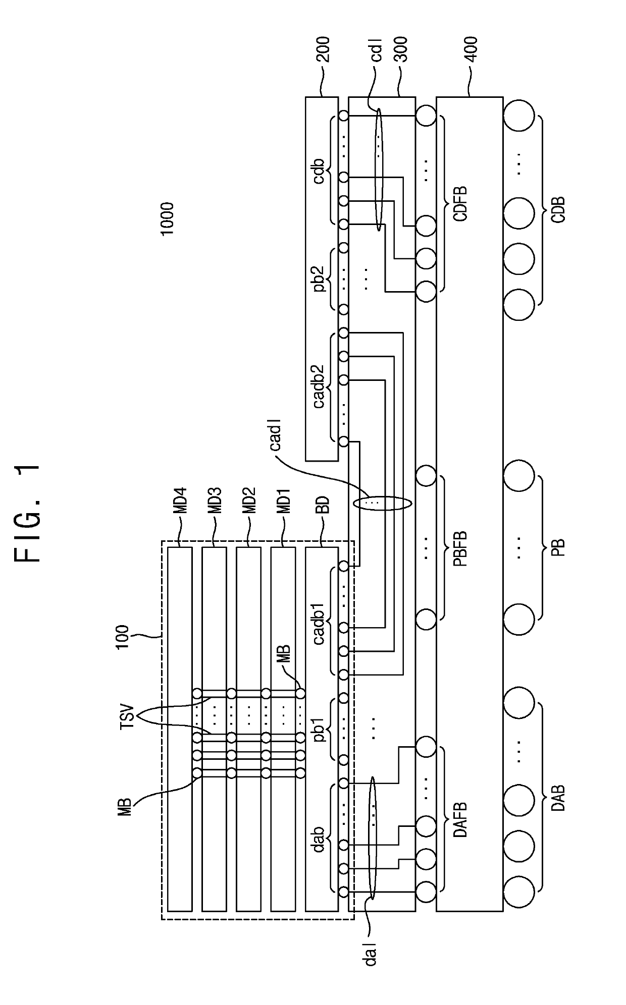
[0025]FIG. 1 is a diagram illustrating a structure of a system device having a 2.5 dimension (D) HBM device according to exemplary embodiments of the present inventive concept, and illustrates a structure of a system device manufactured in a 2.5D package.

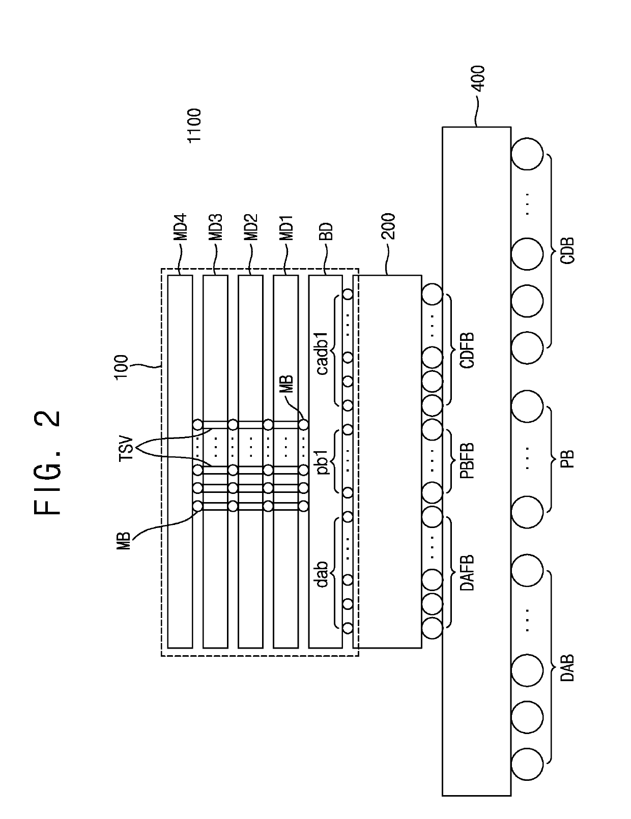
[0026]Referring to FIG. 1, a system device 1000 may include an HBM device 100, a controller 200, an interposer 300, and a printed circuit board (PCB) 400. For example the system device 1000 may be a semiconductor package including a plurality of semiconductor dies mounted on the printed circuit board (PCB) 400, which may be encapsulated by an encapsulant, and the printed circuit board (PCB) 400 may be a package substrate.

[0027]The HBM device 100 may include memory dies MD1 to MD4 and a base die BD (which may be des...


PUM


Abstract

According to some embodiments, a high bandwidth memory device includes a base die and a plurality of memory dies stacked on the base die and electrically connected to the base die through a plurality of through substrate vias. The base die includes a plurality of first input buffers configured to receive channel clock signals, channel command / addresses, and channel data from a plurality of first bumps connected to the outside of the base die, a plurality of second input buffers configured to receive test clock signals, test command / addresses, and test data from a plurality of second bumps connected to the outside of the base die, a monitoring unit, a plurality of first output buffers connected to the monitoring unit and configured to output monitored data from the monitoring unit to the plurality of second bumps, and a plurality of paths from the plurality of first input buffers to the monitoring unit. The plurality of second bumps are connected to receive test clock signals, test command / addresses, and test data from the outside of the base die during a first operation mode, and to receive monitored data from the plurality of first output buffers during a second operation mode.

Description

CROSS-REFERENCE TO RELATED APPLICATION[0001]This U.S. non-provisional patent application claims priority under 35 U.S.C. § 119 to and the benefit of Korean Patent Application No. 10-2018-0028456, filed on Mar. 12, 2018 and Korean Patent Application No. 10-2018-0094449, filed on Aug. 13, 2018, in the Korean Intellectual Property Office (KIPO), the disclosure of which is incorporated herein by reference in its entirety.BACKGROUND1. Field of the Invention[0002]The present inventive concept relates to a high bandwidth memory (HBM) device and a system device having the same.2. Discussion of Related Art[0003]A high bandwidth memory (HBM) device has a structure in which a plurality of memory dies and a base die (which may be described as a buffer die, or a logic die) are stacked. The plurality of memory dies are stacked above the base die, and the plurality of memory dies receive a command / address, for example including command and address bits and in some cases accompanied by data bits, f...

Claims


Application Information

Patent Timeline
IPC IPC(8): G06F3/06G06F13/16G06F12/02G11C7/10
CPCG06F3/0655G06F13/1694G11C7/1057G06F3/0653G11C7/1084G06F12/0292G11C5/063G11C8/06G11C7/222G11C7/225G11C7/1093G11C7/1066G11C2207/2254G11C29/023G11C29/48G11C5/025G11C2029/0409
Inventor LEE, JUN GYUOH, REUMKIM, KI HEUNGOH, MOON HEE
Owner SAMSUNG ELECTRONICS CO LTD
Learn More