TFT substrate, scanning antenna comprising TFT substrate, and method for producing TFT substrate

a scanning antenna and substrate technology, applied in the field of scanning antennas, can solve the problems of high cost and high cost of phased array antennas in the related ar

Active Publication Date: 2019-11-07
SHARP KK
View PDF0 Cites 9 Cited by
  • Summary
  • Abstract
  • Description
  • Claims
  • Application Information

AI Technical Summary

Problems solved by technology

However, phased array antennas in the related art are expensive, which is an obstacle for popularization as a consumer product.
In particular, as the number of antenna units increases, the cost rises considerably.

Method used


Image

  • TFT substrate, scanning antenna comprising TFT substrate, and method for producing TFT substrate
  • TFT substrate, scanning antenna comprising TFT substrate, and method for producing TFT substrate
  • TFT substrate, scanning antenna comprising TFT substrate, and method for producing TFT substrate

Examples


first embodiment

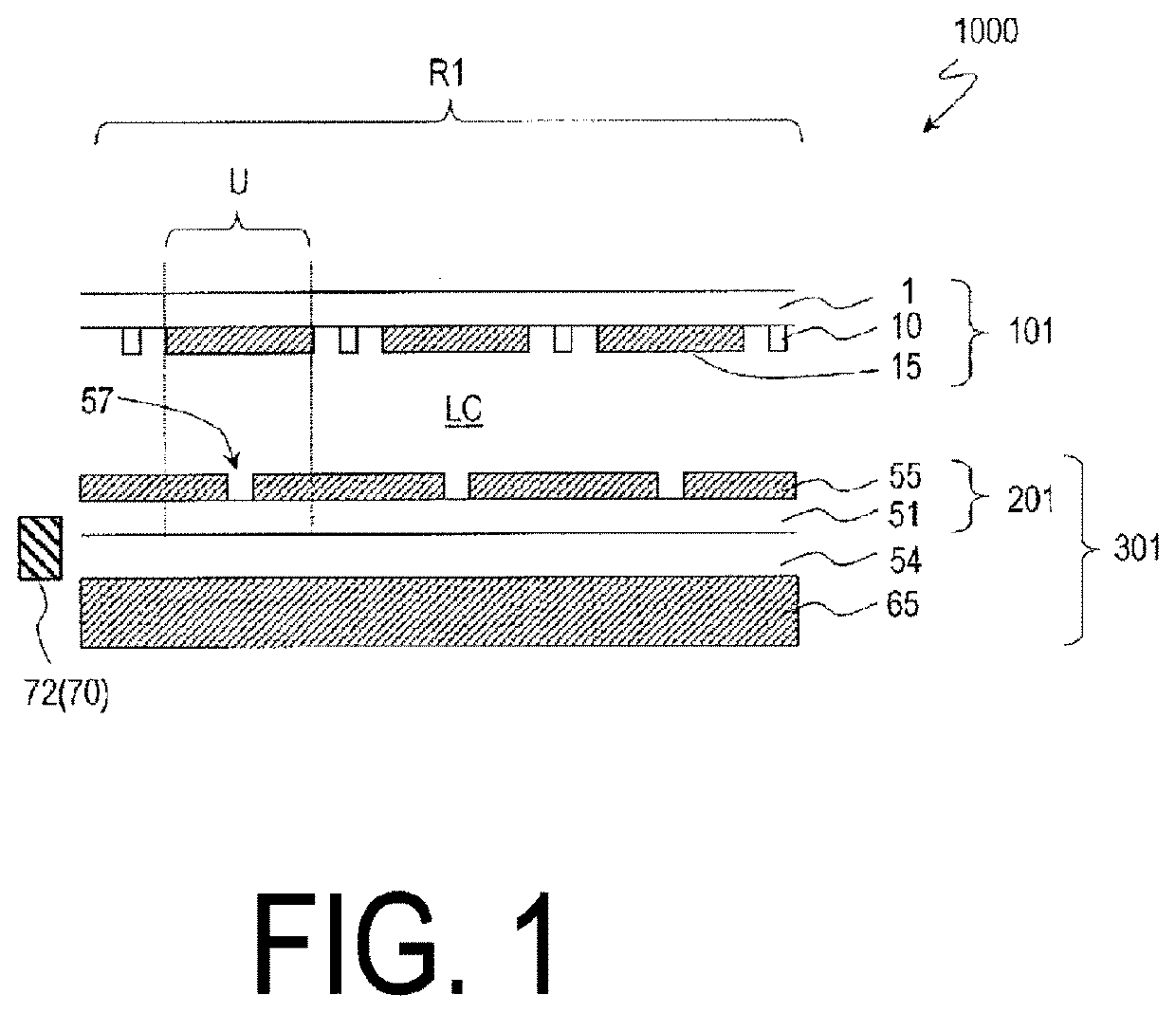
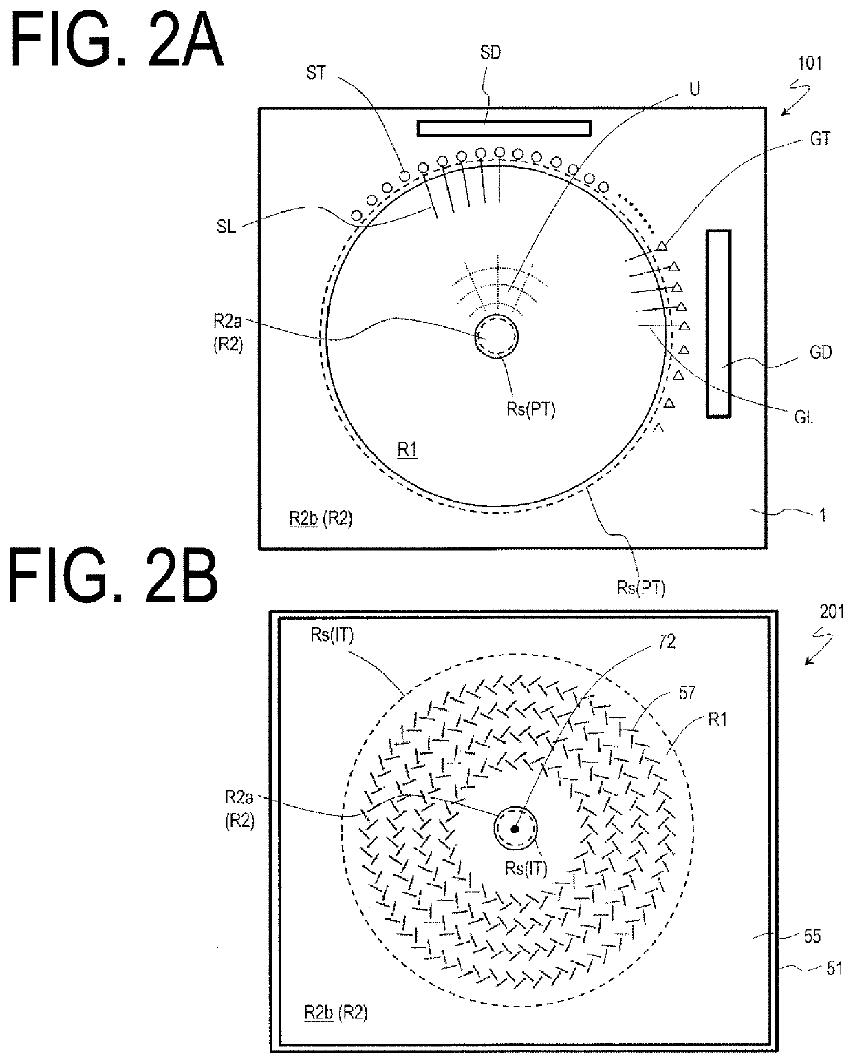
[0101]First, a description is given with reference to FIG. 1 and FIGS. 2A and 2B. FIG. 1 is a schematic partial cross-sectional view of the scanning antenna 1000 near the center thereof as described above, and FIGS. 2A and 2B are schematic plan views illustrating the TFT substrate 101 and the slot substrate 201 in the scanning antenna 1000, respectively.

[0102]The scanning antenna 1000 includes a plurality of antenna units U arranged two-dimensionally. In the scanning antenna 1000 exemplified here, the plurality of antenna units are arranged concentrically. In the following description, the region of the TFT substrate 101 and the region of the slot substrate 201 corresponding to the antenna unit U will be referred to as “antenna unit region,” and be denoted with the same reference numeral U as the antenna unit. In addition, as illustrated in FIGS. 2A and 2B, in the TFT substrate 101 and the slot substrate 201, a region defined by the plurality of two-dimensionally arranged antenna un...

second embodiment

[0190]The scanning antenna of a second embodiment will be described with reference to drawings. The TFT substrate of the scanning antenna of the present embodiment differs from the TFT substrate 101 illustrated in FIG. 2A in that a transparent conductive layer that serves as an upper connection section for each terminal section is provided between the first insulating layer and the second insulating layer of the TFT substrate.

[0191]FIGS. 8A to 8C are cross-sectional views illustrating the gate terminal section GT, the source terminal section ST, and the transfer terminal section PT, respectively, of a TFT substrate 102 in the present embodiment. Constituent elements similar to those in FIGS. 4A to 4C are denoted by the same reference numerals, and the description thereof is omitted. Since the cross-sectional structure of the antenna unit region U is similar to that of the above-described embodiments (FIGS. 3A and 3B), the illustration and description thereof will be omitted.

[0192]Th...

third embodiment

[0206]The scanning antenna of a third embodiment will be described with reference to drawings. The TFT substrate in the scanning antenna of the present embodiment differs from the TFT substrate 102 illustrated in FIGS. 8A to 8C in that the upper connection section made of a transparent conductive film is not provided in the transfer terminal section.

[0207]FIGS. 10A to 10C are cross-sectional views illustrating the gate terminal section GT, the source terminal section ST, and the transfer terminal section PT, respectively, of a TFT substrate 103 in the present embodiment. Constituent elements similar to those in FIGS. 8A to 8C are denoted by the same reference numerals. Since the structure of the antenna unit region U is similar to that of the above-described embodiments (FIGS. 3A and 3B), the illustration and description thereof will be omitted.

[0208]The structures of the gate terminal section GT and the source terminal section ST are similar to the structures of the gate terminal s...


PUM


Abstract

A TFT substrate includes a transmission and / or reception region including a plurality of antenna unit regions, and a non-transmission and / or reception region located in a region other than the transmission and / or reception region. Each of the plurality of antenna unit regions includes a TFT and a patch electrode electrically connected to a drain electrode of the TFT. The TFT substrate includes a source metal layer including a source electrode of the TFT, the drain electrode, and a source bus line, a gate metal layer formed on the source metal layer and including a gate electrode of the TFT and a gate bus line, a gate insulating layer formed between the source metal layer and the gate metal layer, an interlayer insulating layer formed on the gate metal layer, and a conductive layer formed on the interlayer insulating layer. The patch electrode is included in the gate metal layer.

Description

TECHNICAL FIELD[0001]The disclosure relates to a scanning antenna, and more particularly relates to a scanning antenna in which an antenna unit (also referred to as an “element antenna”) has a liquid crystal capacitance (also referred to as a “liquid crystal array antenna”), a TFT substrate used for such a scanning antenna, and a manufacturing method of such a TFT substrate.BACKGROUND ART[0002]Antennas for mobile communication and satellite broadcasting require functions that can change the beam direction (referred to as “beam scanning” or “beam steering”). As an example of an antenna (hereinafter referred to as a “scanning antenna” (scanned antenna) having such functionality, phased array antennas equipped with antenna units are known. However, phased array antennas in the related art are expensive, which is an obstacle for popularization as a consumer product. In particular, as the number of antenna units increases, the cost rises considerably.[0003]Therefore, scanning antennas th...

Claims


Application Information

Patent Timeline
Patent Type & Authority Applications(United States)
IPC IPC(8): H01Q3/34H01Q21/06H01L23/66
CPCH01L23/66G02F1/1368H01Q21/061H01Q3/34H01L2223/6677H01Q3/44H01L29/786H01Q21/0012H01Q21/064
Inventor MISAKI, KATSUNORI
Owner SHARP KK
Why Eureka
Try Eureka