Scanned antenna and method for manufacturing same

一种扫描天线、制造方法的技术,应用在扫描天线领域,能够解决成本上升、相控阵列天线价格高等问题

Active Publication Date: 2018-08-21
SHARP KK
View PDF14 Cites 11 Cited by
  • Summary
  • Abstract
  • Description
  • Claims
  • Application Information

AI Technical Summary

Problems solved by technology

However, the high price of existing phased array antennas has become an obstacle to the popularization of consumer products
In particular, when the number of antenna units increases, the cost rises significantly

Method used


Image

  • Scanned antenna and method for manufacturing same
  • Scanned antenna and method for manufacturing same
  • Scanned antenna and method for manufacturing same

Examples


no. 1 approach

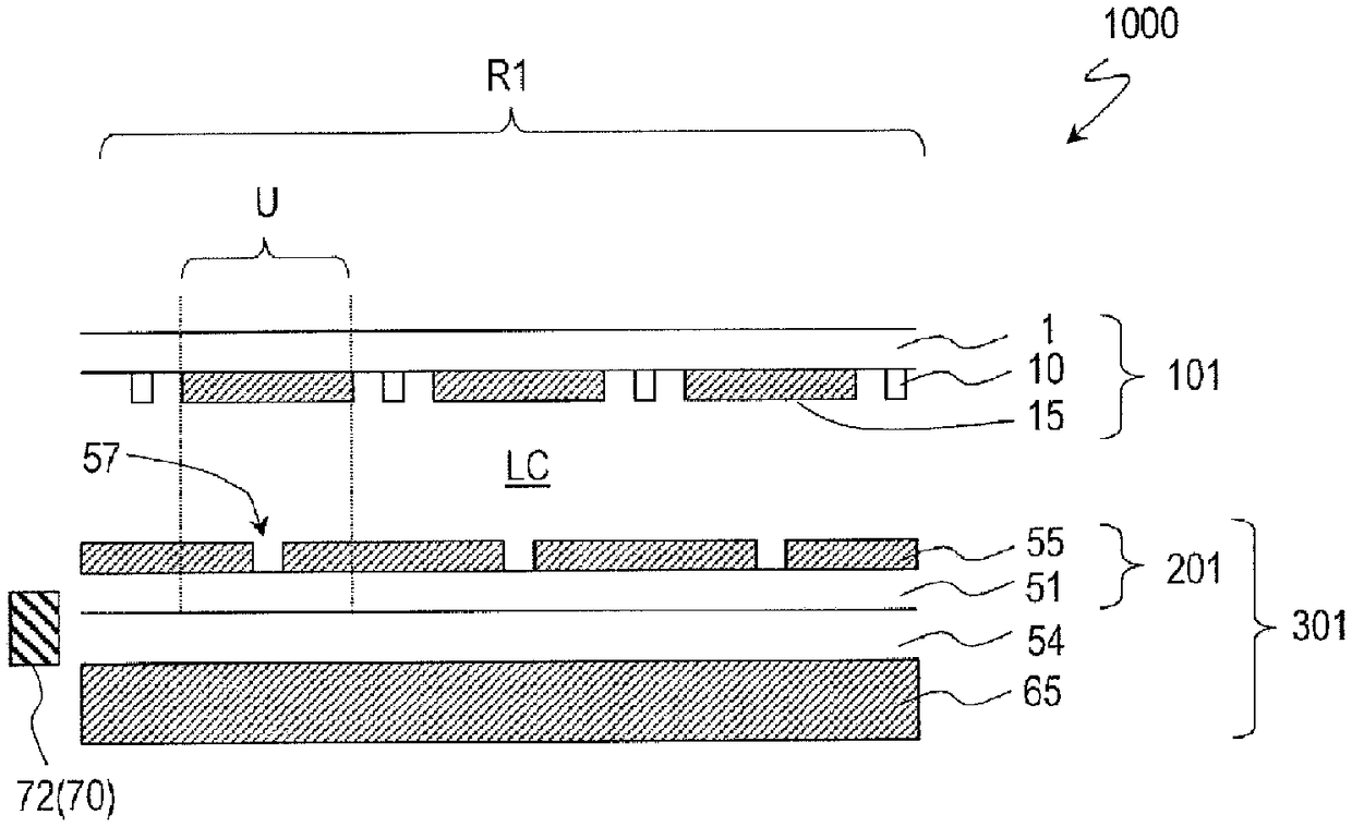
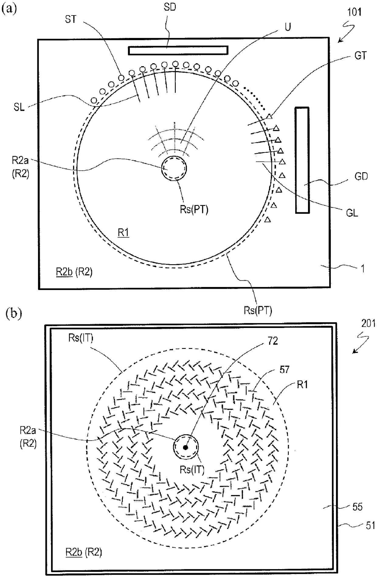
[0119] First, refer to figure 1 with figure 2 . figure 1 As described in detail, it is a schematic partial cross-sectional view near the center of the scanning antenna 1000, figure 2 (A) and (b) are schematic plan views showing the TFT substrate 101 and the slot substrate 201 in the scanning antenna 1000, respectively.

[0120] The scanning antenna 1000 has a plurality of antenna units U arranged in two dimensions. In the scanning antenna 1000 illustrated here, the plurality of antenna units are arranged in concentric circles. In the following description, the area of ​​the TFT substrate 101 and the area of ​​the slot substrate 201 corresponding to the antenna unit U are referred to as "antenna unit area", and the same reference sign U as the antenna unit is given. In addition, such as figure 2 As shown in (a) and (b), in the TFT substrate 101 and the slot substrate 201, the area defined by a plurality of antenna unit areas arranged two-dimensionally is called the "transmissi...

no. 2 approach

[0213] The scanning antenna of the second embodiment will be described with reference to the drawings. The TFT substrate in the scanning antenna of this embodiment and the figure 2 The difference of the TFT substrate 101 shown is that the transparent conductive layer which becomes the upper connection part of each terminal part is provided between the first insulating layer and the second insulating layer in the TFT substrate.

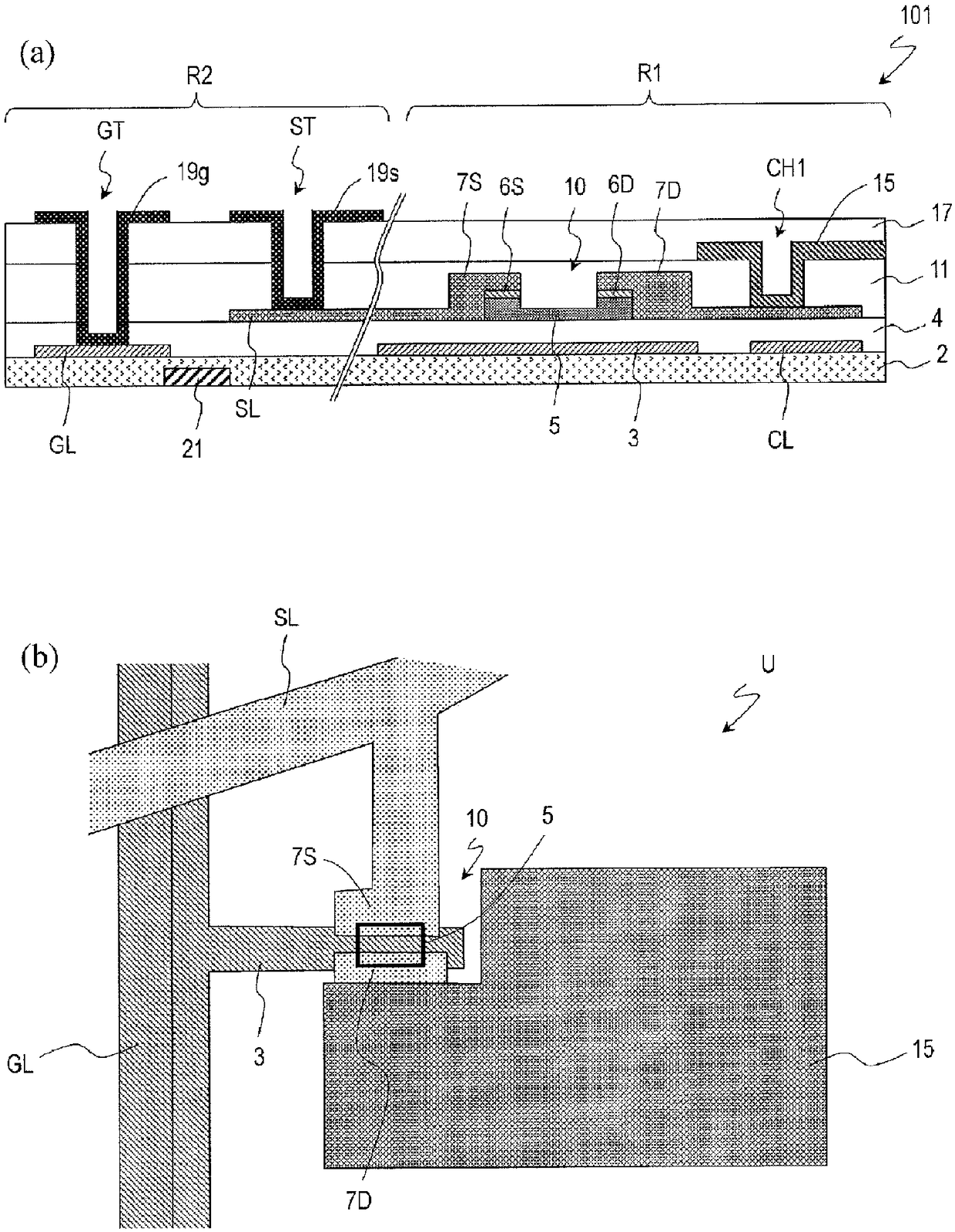
[0214] Figure 8 (a) to (c) are respectively cross-sectional views showing the gate terminal portion GT, the source terminal portion ST, and the transmission terminal portion PT of the TFT substrate 102 in this embodiment. Right and Figure 4 The same components are denoted by the same reference numerals, and the description is omitted. In addition, the cross-sectional structure of the antenna unit area U is the same as the above-mentioned embodiment ( image 3 ) Are the same, so the illustration and description are omitted.

[0215] The gate terminal por...

no. 3 approach

[0231] The scanning antenna of the third embodiment will be described with reference to the drawings. The TFT substrate in the scanning antenna of this embodiment and the Figure 8 The difference of the TFT substrate 102 shown is that the upper connection portion made of a transparent conductive film is not provided in the transmission terminal portion.

[0232] Picture 10 (a) to 10(c) are respectively cross-sectional views showing the gate terminal portion GT, the source terminal portion ST, and the transmission terminal portion PT of the TFT substrate 103 in this embodiment. Right and Figure 8 The same components are denoted by the same reference numerals, and the description is omitted. In addition, the structure of the antenna unit area U is the same as the above-mentioned embodiment ( image 3 ) Are the same, so the illustration and description are omitted.

[0233] The structure of the gate terminal GT and the source terminal ST Figure 8 The gate terminal portion and sour...


PUM

PropertyMeasurementUnit
electrical resistivityaaaaaaaaaa
visible light transmittanceaaaaaaaaaa
viscosity indexaaaaaaaaaa

Abstract

A scanned antenna (1000) is a scanned antenna in which antenna units U are arranged and which comprises: a first dielectric substrate (1); a TFT substrate (101) including TFTs, gate bus lines, sourcebus lines, and patch electrodes (15); a slot substrate (201) including a second dielectric substrate (51) and a slot electrode (55) formed on a first main surface of the second dielectric substrate; aliquid crystal layer LC provided between the TFT substrate and the slot substrate; and a reflective conductor plate (65) disposed so as to oppose , across a dielectric layer (54), a second main surface of the second dielectric substrate (51) on the opposite side from the first main surface. The slot electrode includes slots disposed corresponding to each of the patch electrodes, and the second dielectric substrate (51) and the slot electrode (55) have an adhesive layer (92) formed therebetween from a heat-curable or photo-curable adhesive material.

Description

Technical field [0001] The present invention relates to a scanning antenna, and in particular to a scanning antenna (sometimes called a "liquid crystal array antenna") having a liquid crystal capacitor in an antenna unit (sometimes called a "dipole antenna") and a manufacturing method thereof. Background technique [0002] Antennas used for mobile communication and satellite broadcasting need to be able to change the direction of the beam (called "beam scanning" or "beam steering"). As an antenna having such a function (hereinafter, referred to as "scanned antenna"), a phased array antenna having an antenna unit is known. However, the existing phased array antennas are expensive and become an obstacle to popularization of consumer products. In particular, when the number of antenna units increases, the cost increases significantly. [0003] Therefore, scanning antennas using the large dielectric anisotropy (birefringence) of liquid crystal materials (including nematic liquid crys...

Claims


Application Information

Patent Timeline
Patent Type & Authority Applications(China)
IPC IPC(8): H01Q3/34G02F1/13H01Q3/44H01Q13/22
CPCG02F1/13H01L27/1255H01Q3/36H01Q3/44H01Q9/0457H01Q21/0012H01Q21/065G02F1/1368H01L27/1262H01Q13/22H01Q21/005
Inventor 高桥纯平水崎真伸箕浦洁坂井彰
Owner SHARP KK
Why Eureka
Try Eureka