Antenna device and communication apparatus using the same

a technology of communication apparatus and antenna device, which is applied in the structure of radiating elements, elongated active elements, and resonant antennas. it can solve the problems of enlarging the size of the antenna device as a whole, preventing the acquisition of desired characteristics, and affecting the success of communication apparatus downsizing,

Inactive Publication Date: 2001-08-28
MURATA MFG CO LTD
View PDF4 Cites 129 Cited by
  • Summary
  • Abstract
  • Description
  • Claims
  • Application Information

AI Technical Summary

Problems solved by technology

However, in such type of antenna devices, too small a space between two patch antennas 101 and 102 tends to develop undesirable interference between the two patch antennas, preventing obtaining desired characteristics.
This presents a problem of enlarging the size of the antenna device as a whole.
Recently, downsizing of communication apparatus such as a mobile telephone using the antenna device has been promoted and the configuration of two patch antennas disposed side-by-side will present difficulty for further promotion o

Method used


Image

  • Antenna device and communication apparatus using the same
  • Antenna device and communication apparatus using the same
  • Antenna device and communication apparatus using the same

Examples


first embodiment

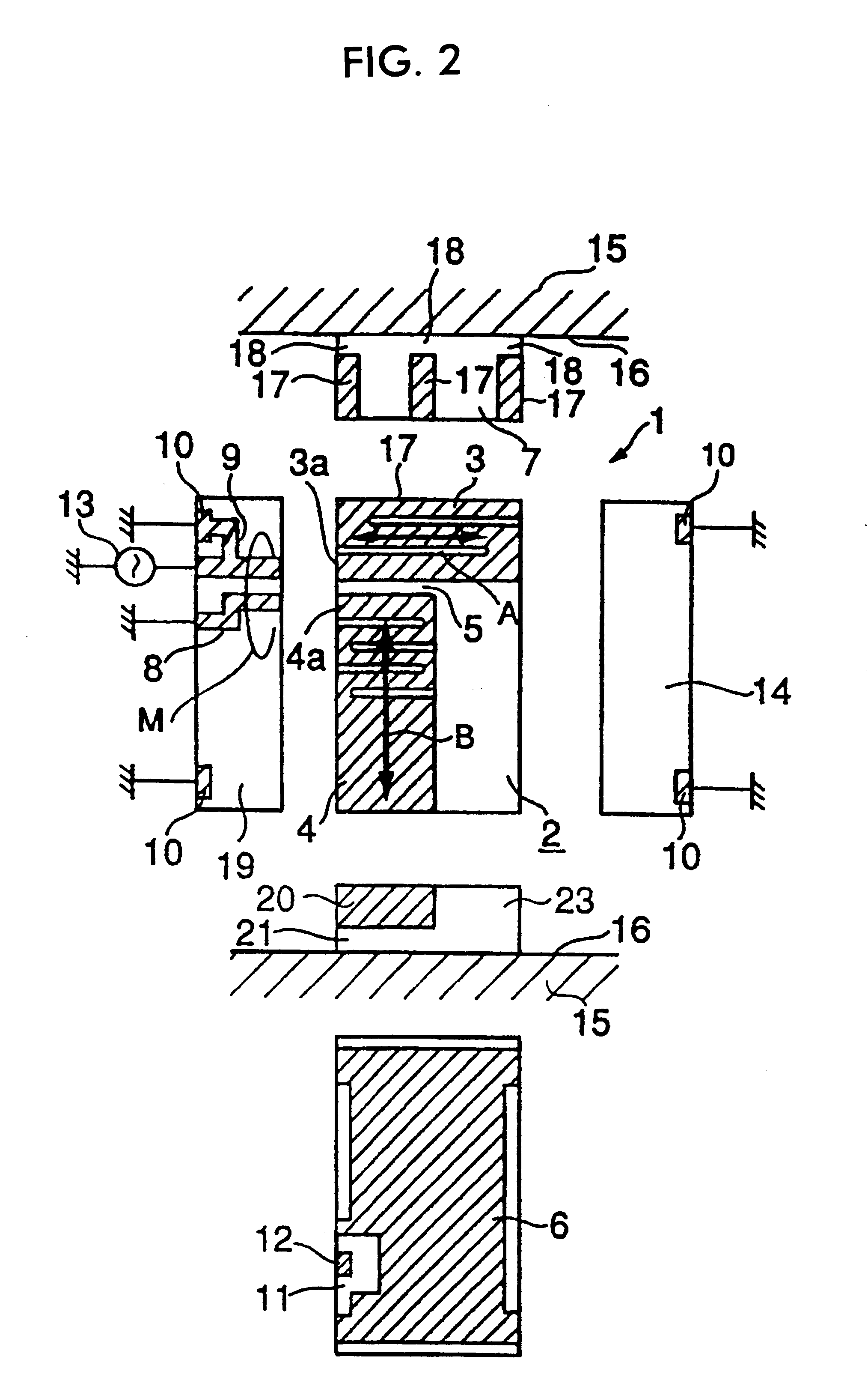
FIG. 1 schematically shows the configuration of the antenna device of the present invention. The 6 views in FIG. 1 schematically show the surfaces of the dielectric substrate 1 over which various electrodes are formed.

In FIG. 1 a dielectric substrate 1 is formed of such a material as ceramics, resin or the like with a high dielectric constant in the shape of a rectangular solid. On the top surface 2 of the dielectric substrate 1 are formed a feeding radiation electrode 3 and a non-feeding radiation electrode 4 in a meandering shape, respectively. The non-feeding radiation electrode 4 is formed over a quadrilateral area along a longer edge on the left-hand side of the rectangular top surface 2. The quadrilateral area extends over the whole length of the longer edge on the left-hand side of the top surface 2. The feeding radiation electrode 3 is formed over a quadrilateral area including a corner of a shorter edge on the upper right hand side of the top surface 2. The non-feeding radi...

fourth embodiment

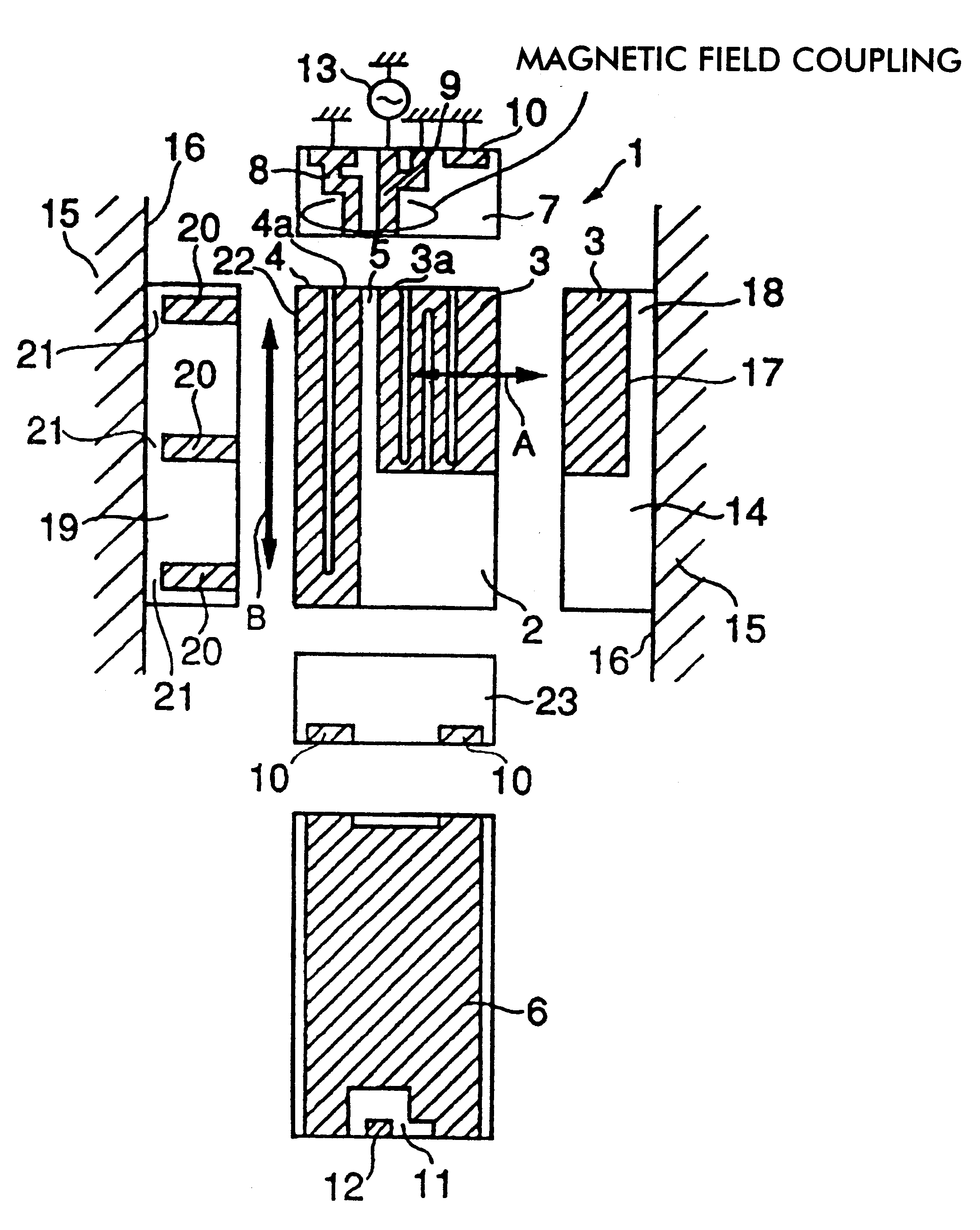
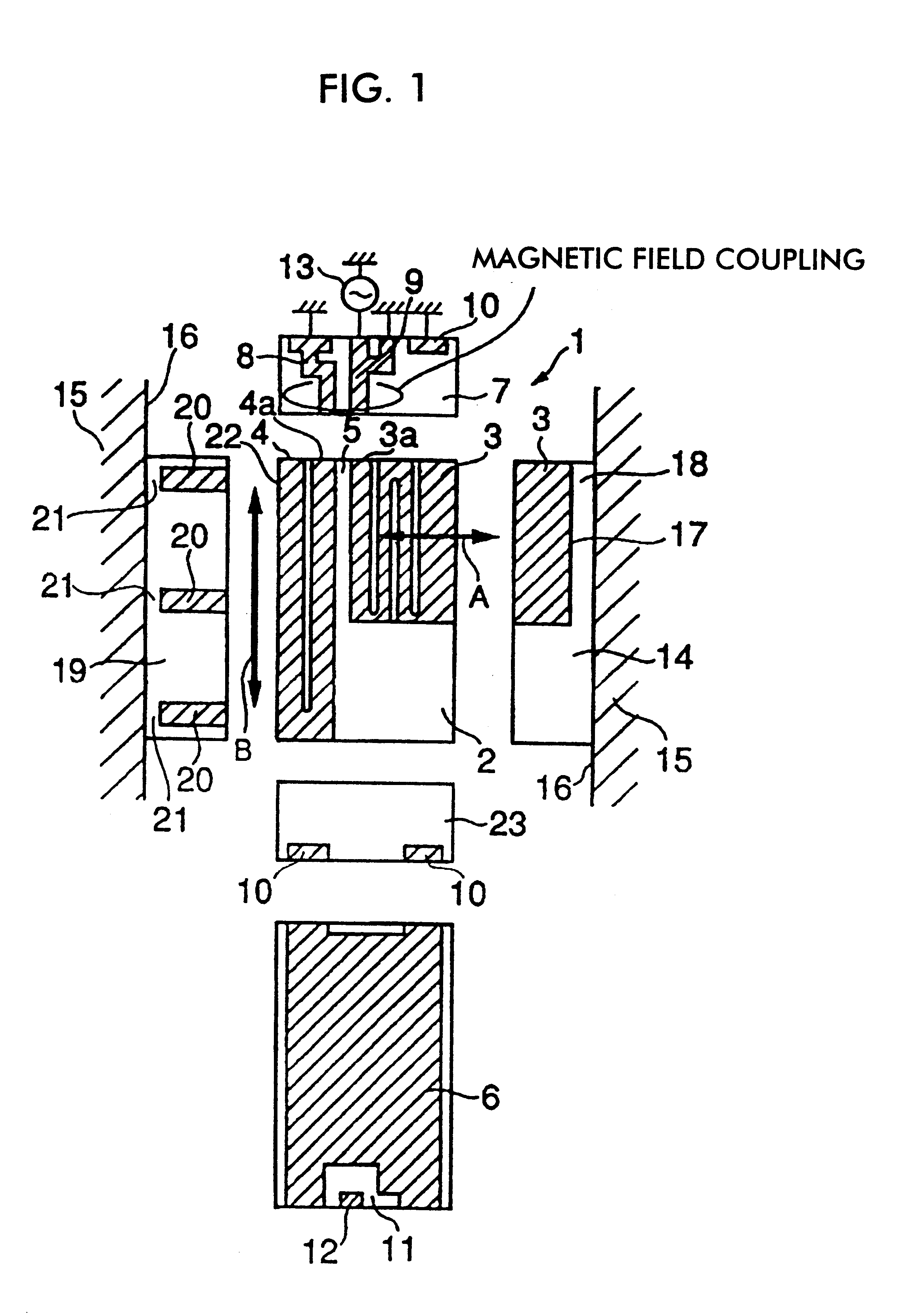
Also, in the fourth embodiment, as the open end 17 of the feeding radiation electrode 3 is formed on the right side surface 14 of the dielectric substrate 1 and the open end (the open-end electrode 20) of the non-feeding radiation electrode 4 is formed on the rear side surface 23, the open ends of the feeding radiation electrode 3 and the non-feeding radiation electrode 4 are formed on the mutually perpendicular different sides 14 and 23. As a result, it is possible to prevent mutual signal interference between high intensity electric field portions of the feeding radiation electrode 3 and the non-feeding radiation electrode 4 substantially completely.

Also, both of the short-circuit part 8 and the short-circuit part 9 on the left side surface 19 of the dielectric substrate 1 are arranged to connect to the ground surface 16 of the mounting board 15. In the fourth embodiment, similar to the third embodiment above, a signal supplied from the signal source 13 is fed by capacitance coupl...


PUM


Abstract

An antenna device comprising: a feeding radiation electrode and a non-feeding radiation electrode separately disposed on a surface of a dielectric substrate; a short circuit part of the feeding radiation electrode and a short circuit part of the non-feeding radiation electrode adjacently disposed to each other on one side surface of the dielectric substrate; and an open end of the feeding radiation electrode and an open end of the non-feeding radiation electrode disposed on mutually different surface sides of the dielectric substrate other than the surface on which said short circuit parts are disposed.

Description

1. Field of the InventionThe present invention relates to a surface-mount antenna device that allows communication in two frequency bands and a communication apparatus such as a mobile telephone that uses the same.2. Description of the Related ArtFIG. 9 shows a conventional antenna device that is adapted to communication in two frequency bands. In FIG. 9 an antenna device 100 comprises two patch antennas 101 and 102 that have different resonant frequencies and are disposed side-by-side with a certain spacing to allow both of them to be connected to a single signal source 103 via capacitance coupling. It is thus possible to construct an antenna device that responds to two frequency bands by disposing two patch antennas with different resonant frequencies side-by-side.However, in such type of antenna devices, too small a space between two patch antennas 101 and 102 tends to develop undesirable interference between the two patch antennas, preventing obtaining desired characteristics. I...

Claims


Application Information

Patent Timeline
IPC IPC(8): H01Q5/00H01Q19/00H01Q9/04H01Q1/24H01Q19/26H01Q1/38H01Q9/42H01Q13/08H01Q13/26H01Q21/30H04B1/38
CPCH01Q1/243H01Q5/378H01Q19/005H01Q9/0421H01Q13/26
Inventor NAGUMO, SHOJITSUBAKI, NOBUHITOKAWAHATA, KAZUNARI
Owner MURATA MFG CO LTD
Why Eureka
Try Eureka