Scanning antenna
A technology for scanning antennas and antennas, applied in the field of scanning antennas, can solve the problems of rising costs and high prices of phased array antennas
- Summary
- Abstract
- Description
- Claims
- Application Information
AI Technical Summary
Problems solved by technology
Method used
Image
Examples
no. 1 Embodiment approach
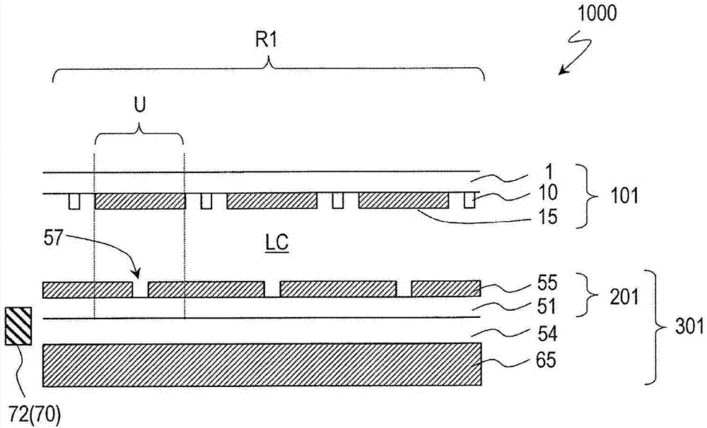
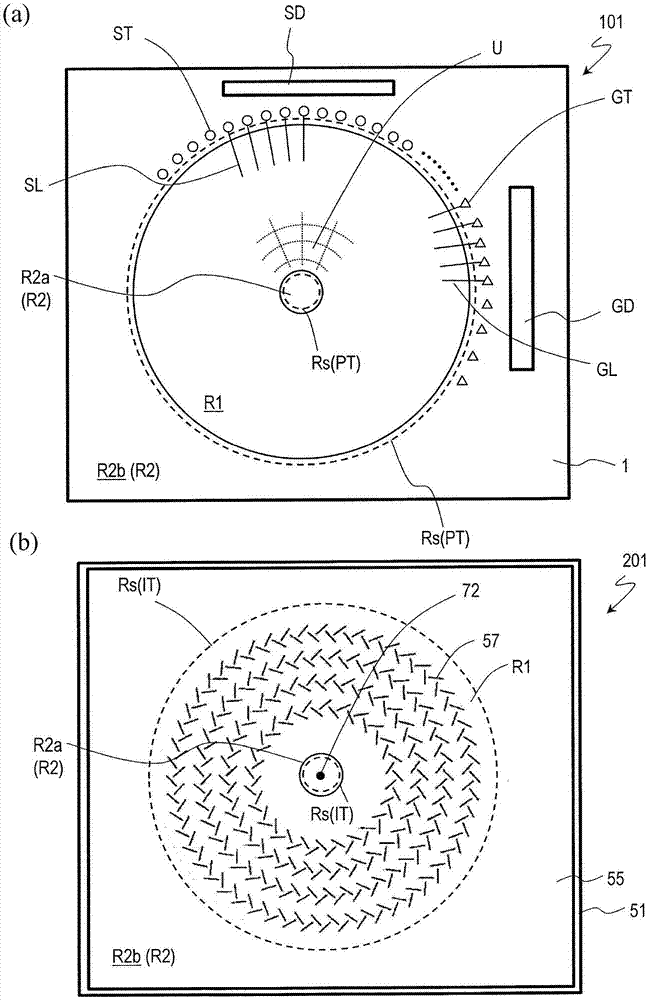
[0117] First, refer to figure 1 and figure 2 . figure 1 As described in detail, it is a schematic partial cross-sectional view near the center of the scanning antenna 1000, figure 2 (a) and figure 2 (b) are schematic plan views showing the TFT substrate 101 and the slot substrate 201 in the scanning antenna 1000, respectively.
[0118] The scanning antenna 1000 has a plurality of antenna units U arranged two-dimensionally, and in the scanning antenna 1000 illustrated here, the plurality of antenna units are arranged concentrically. In the following description, the region of the TFT substrate 101 and the region of the slot substrate 201 corresponding to the antenna unit U are referred to as "antenna unit region", and the same reference numeral U as that of the antenna unit is assigned. Additionally, if figure 2 (a) and figure 2 As shown in (b), in the TFT substrate 101 and the slot substrate 201, the area defined by a plurality of antenna unit areas arranged two-d...
no. 2 Embodiment approach
[0211] A scanning antenna according to a second embodiment will be described with reference to the drawings. The TFT substrate in the scanning antenna of this embodiment and figure 2 The TFT substrate 101 shown is different in that a transparent conductive layer serving as an upper connection portion of each terminal portion is provided between the first insulating layer and the second insulating layer in the TFT substrate.
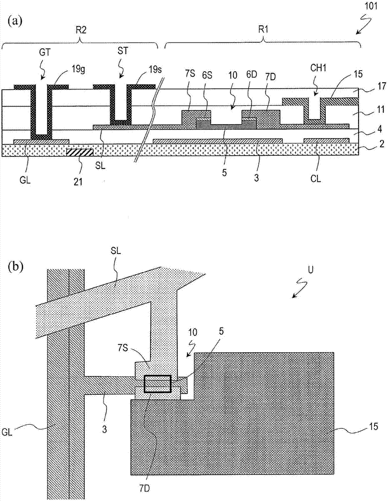
[0212] Figure 8 (a)~ Figure 8 (c) is a cross-sectional view showing the gate terminal portion GT, the source terminal portion ST, and the transmission terminal portion PT of the TFT substrate 102 according to the present embodiment, respectively. right with Figure 4 The same components are denoted by the same reference numerals, and description thereof will be omitted. In addition, the cross-sectional structure of the antenna unit area U is the same as the above-mentioned embodiment ( image 3 ) are the same, so illustrations and descriptions are...
no. 3 Embodiment approach
[0229] A scanning antenna according to a third embodiment will be described with reference to the drawings. The TFT substrate in the scanning antenna of this embodiment and Figure 8 The illustrated TFT substrate 102 is different in that an upper connection portion including a transparent conductive film is not provided to the transmission terminal portion.
[0230] Figure 10 (a)~ Figure 10 (c) is a cross-sectional view showing the gate terminal portion GT, the source terminal portion ST, and the transmission terminal portion PT of the TFT substrate 103 according to the present embodiment, respectively. right with Figure 8 The same components are denoted by the same reference numerals, and description thereof will be omitted. In addition, the structure of the antenna unit area U is the same as that of the above-mentioned embodiment ( image 3 ) are the same, so illustrations and descriptions are omitted.
[0231] The structure of the gate terminal part GT and the sour...
PUM
| Property | Measurement | Unit |
|---|---|---|
| electrical resistivity | aaaaa | aaaaa |
| visible light transmittance | aaaaa | aaaaa |
| contact resistance | aaaaa | aaaaa |
Abstract
Description
Claims
Application Information


