Method for 3D waveform mapping of full-parallel structure

Active Publication Date: 2019-12-26
UNIV OF ELECTRONIC SCI & TECH OF CHINA
View PDF1 Cites 0 Cited by
  • Summary
  • Abstract
  • Description
  • Claims
  • Application Information

AI Technical Summary

Benefits of technology

The present invention provides a method for faster and more efficient mapping of full-parallel structures using 3D waveform mapping. By creating a database and dividing it into smaller sections, a parallel mapping process can be performed simultaneously on the time and amplitude axes using multiple RAMs. This reduces mapping time, especially in vector mapping mode, and improves the WCR of DSO.

Problems solved by technology

The processes of the conventional 3D waveform mapping are simple, however, the time consumption is heavy, which greatly limits the improvement of WCR.
However, in vector mapping mode, when mapping a complex signal which has an amplitude difference of 2N (N is the resolution of ADC) at two consecutive time points, a mapping of 2N sampling values is needed at a time point, which leads to a sharp time increase in the vector mapping for one frame of waveform.

Method used


Image

  • Method for 3D waveform mapping of full-parallel structure
  • Method for 3D waveform mapping of full-parallel structure
  • Method for 3D waveform mapping of full-parallel structure

Examples


embodiment

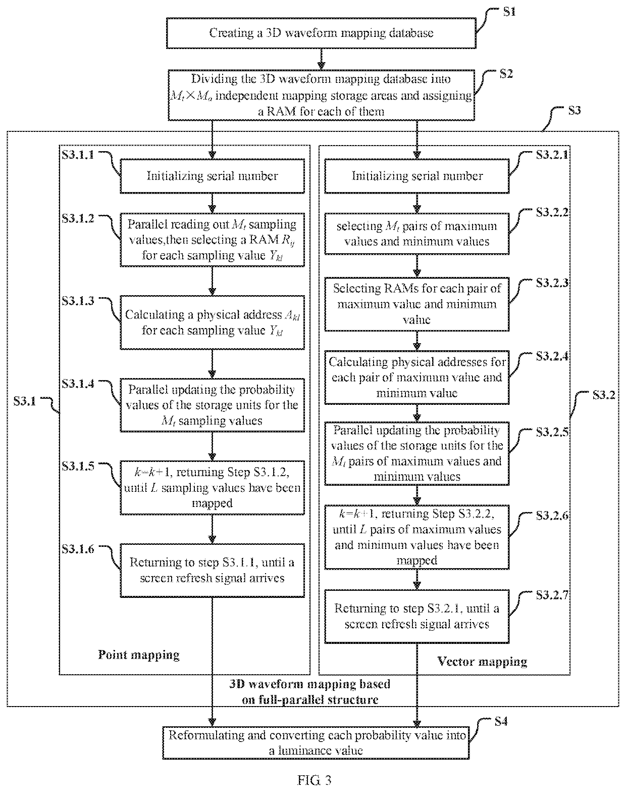
[0049]FIG. 3 is a flow diagram of a method for 3D waveform mapping of full-parallel structure in accordance with the present invention.

[0050]In one embodiment, As shown in FIG. 3, a method for 3D waveform mapping of full-parallel structure comprises the following steps:

[0051]Step S1: creating a 3D waveform mapping database, where the size of the 3D waveform mapping database is L×2N×B / 8 (byte), L and 2N are respectively the length and the width of a 3D waveform image, B is the number of bits of probability value, N is the ADC's resolution of a data acquisition module.

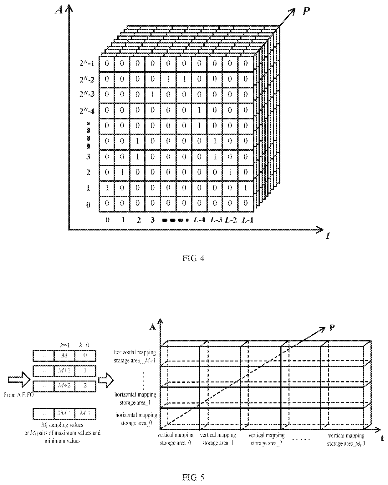
[0052]As shown in FIG. 4, a typical 3D waveform image has L sampling points along the time axis t. The amplitude of each sampling point, i.e. sampling value is between 0 and 2N, N is the ADC's resolution of a data acquisition module which acquired the sampling values, thus the length and the width of the 3D waveform image are L and 2N respectively. A dot on 3D waveform image is the number of occurrences, i.e. probability...


PUM


Abstract

The present invention provides a method for 3D waveform mapping of full-parallel structure, first, a 3D waveform mapping database is created according to the size of a 3D waveform image, the number of bits of probability value and the ADC's resolution of data acquisition module, then the 3D waveform mapping database is divided into Mt×Ma independent mapping storage areas along the time axis and the amplitude axis, and each independent mapping storage area is assigned a RAM, then RAMs are selected and addresses are calculated based on the sampling values and the structure of created 3D waveform mapping database, finally, parallel mappings are performed simultaneously on the time axis and the amplitude axis according to the selected RAMs and calculated addresses. Thus, the mapping time are shorten, especially in vector mapping mode, several RAMs are used for mapping, so the WCR of DSO is improved.

Description

FIELD OF THE INVENTION[0001]This application claims priority under the Paris Convention to Chinese Patent Application No. 201810643986.2, filed on Jun. 21, 2018, the entirety of which is hereby incorporated by reference for all purposes as if fully set forth herein.[0002]The present invention relates to the field of waveform display, more particularly to a method for 3D waveform mapping of full-parallel structure.BACKGROUND OF THE INVENTION[0003]Three-dimensional (3D) waveform display is one of the main functions of 3D digital storage oscilloscope (DSO). 3D waveform image displayed on screen can provide not only the time information and the amplitude information of a waveform, but also the occurrences (probability) information of the waveform, which is indicated by different levels of luminance. Usually, 3D waveform display is realized through 3D waveform mapping, which improves the waveform capture rate (WCR) of DSO. WRC is one of the key performance specifications of DSO. The high...

Claims


Application Information

Patent Timeline
IPC IPC(8): G06T1/60G06F16/22G06F3/06G06T11/20G01R13/02
CPCG06F3/0604G06T11/206G06F3/0659G01R13/029G01R13/0272G06T1/60G06T2200/28G06F16/2264G06F3/0673G01R13/0209G06F3/05G06F5/06G01R13/0227G01R13/0236G01R13/206
Inventor HUANG, WUHUANGWANG, PANJIANG, JUNYE, PENGYANG, KUOJUNGUO, LIANPINGZENG, HAOWANG, SHUOGAO, JIAN
Owner UNIV OF ELECTRONIC SCI & TECH OF CHINA
Why Eureka
Try Eureka