Cleaning device and method for driving cleaning device

a cleaning device and cleaning technology, applied in the direction of basic electric elements, semiconductor/solid-state device manufacturing, electric devices, etc., can solve the problems of increasing the defect rate of semiconductor devices, reducing the manufacturing yield, and generating contaminants, so as to prevent or minimize contaminants

Active Publication Date: 2020-06-25
SAMSUNG ELECTRONICS CO LTD
View PDF0 Cites 2 Cited by
  • Summary
  • Abstract
  • Description
  • Claims
  • Application Information

AI Technical Summary

Benefits of technology

[0006]Aspects of the present disclosure provide a cleaning device including a plurality of cleaning modules for cleaning the wafer after chemical mechanical polishing (CMP), which prevents or minimizes contaminants generated in a cleaning module of the initial stage from being transferred to a cleaning module of a later stage, and a method for driving the cleaning device.

Problems solved by technology

However, when a single blade performs an operation of inserting or removing wafers into and out from a plurality of cleaning modules, there may be a problem in which contaminants generated in the cleaning module corresponding to the initial stage are transferred to a cleaning module corresponding to a later stage (or a drying module).
This may result in a decrease in a manufacturing yield and an increase in a defect rate of the semiconductor devices.

Method used


Image

  • Cleaning device and method for driving cleaning device
  • Cleaning device and method for driving cleaning device
  • Cleaning device and method for driving cleaning device

Examples


Embodiment Construction

[0024]Hereinafter, various embodiments of the present disclosure will be described with reference to the accompanying drawings.

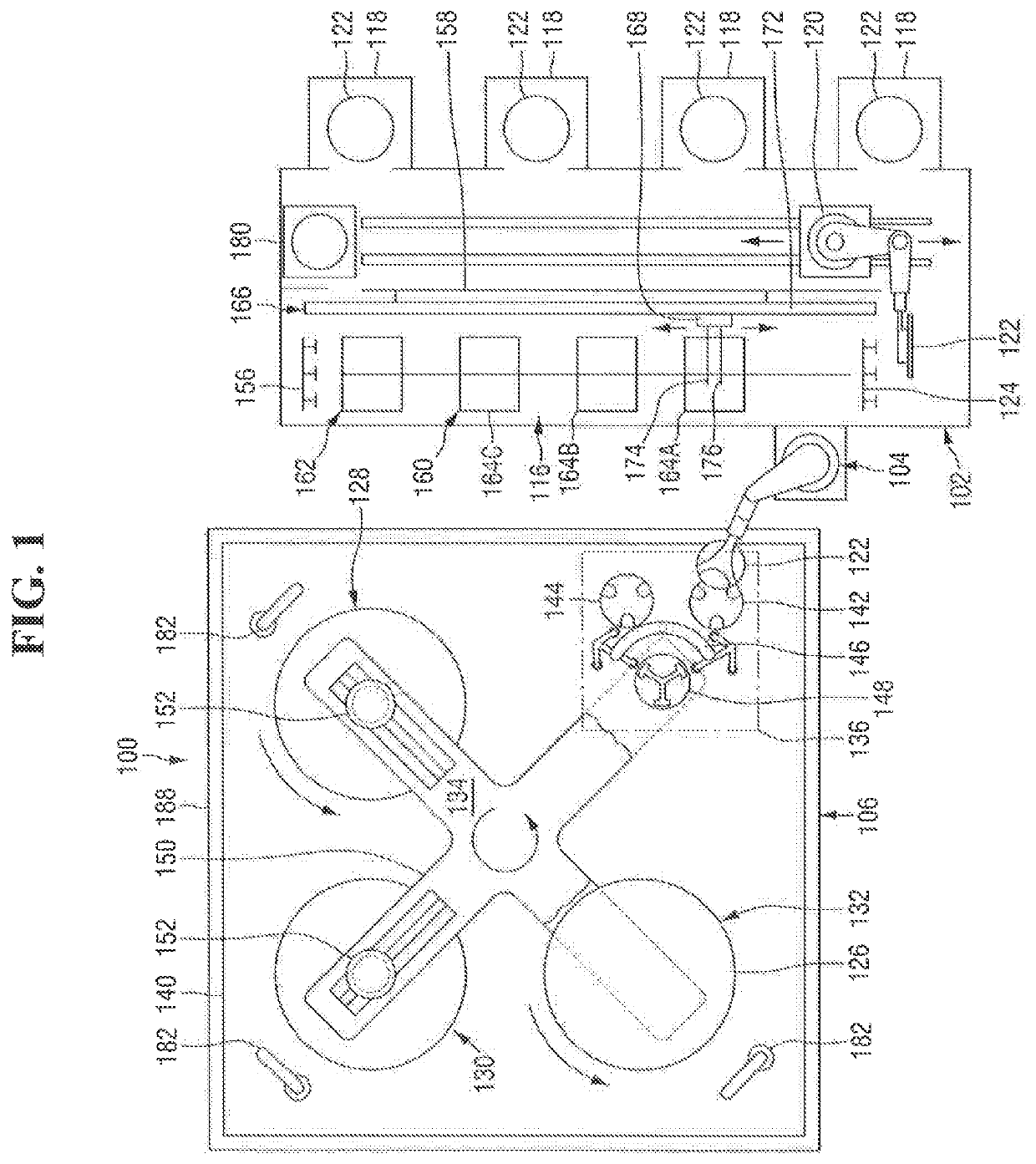
[0025]FIG. 1 is a diagram illustrating a chemical mechanical polishing system according to an embodiment of the present disclosure.

[0026]Referring to FIG. 1, a chemical mechanical polishing system 100 according to an embodiment of the present disclosure includes a factory interface 102, a loading unit 104 and a planarization unit 106. The loading unit 104 is located between the factory interface 102 and the planarization unit 106 to perform the transfer of the wafer 122 between them.

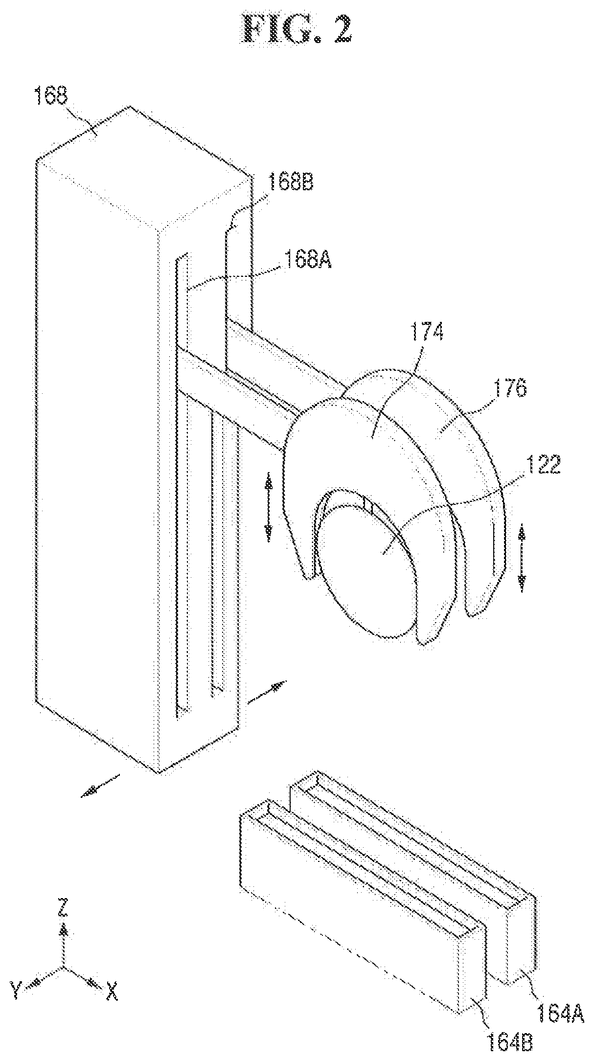
[0027]The factory interface 102 includes a cleaning device 116 and one or more cassettes 118. The interface unit 120 performs the transfer of the wafer 122 between the cassette 118 and the cleaning device 116 (especially, an input module 124).

[0028]The planarization unit 106 includes one or more chemical mechanical polishing stations 128, 130 and 132 inside an enclosure 188. As a...


PUM


Abstract

Provided are a cleaning device and a method for driving the cleaning device which cleans a wafer after chemical mechanical polishing. The cleaning device includes a cleaning modules and a running beam, the running beam including a first blade and a second blade to insert or remove the wafer with respect to one of the cleaning modules in a second direction, the first blade and the second blade being fixed to the running beam and movable in the second direction, and the cleaning modules including an input module, a megasonic module, a first brush module, a second brush module and a drying module. The driving method includes performing an operation of inserting or removing the wafer in the second direction using the first blade in a first area; and performing an operation of inserting or removing the wafer in the second direction using the second blade in a second area.

Description

CROSS-REFERENCE TO RELATED APPLICATION[0001]This application claims the benefit of Korean Patent Application No. 10-2018-0168234, filed on Dec. 24, 2018, in the Korean Intellectual Property Office, the disclosure of which is incorporated by reference herein in its entirety.BACKGROUND1. Field of the Disclosure[0002]The present disclosure relates to a cleaning device which cleans a wafer after chemical mechanical polishing (CMP) and a method for driving the cleaning device.2. Description of the Related Art[0003]Equipment used in chemical mechanical polishing includes a polishing device which polishes a wafer, and a cleaning device which cleans the wafer after polishing. The cleaning device includes a plurality of cleaning modules disposed therein in a plurality of stages, and a wafer may be cleaned and dried while going through the aforementioned stages.[0004]The cleaning device conveys the wafer between a plurality of cleaning modules, using a running beam, and the running beam may b...

Claims


Application Information

Patent Timeline
Patent Type & Authority Applications(United States)
IPC IPC(8): H01L21/02H01L21/67H01L21/687
CPCH01L21/02074H01L21/67034H01L21/68707H01L21/67046H01L21/67051H01L21/67173H01L21/67219H01L21/67751H01L21/67757H01L21/67766H01L21/02096H01L21/304H01L21/67092H01L21/67242H01L21/78H01L21/67028H01L21/67703H01L21/67736H01L21/67739
Inventor PARK, HYUN JOONKIM, JIN YONGPARK, BONG KLPARK, EUN SUNSEO, JAE HYEONLEE, YOUNG CHUL
Owner SAMSUNG ELECTRONICS CO LTD
Why Eureka
Try Eureka