Microled display and a method of forming the same

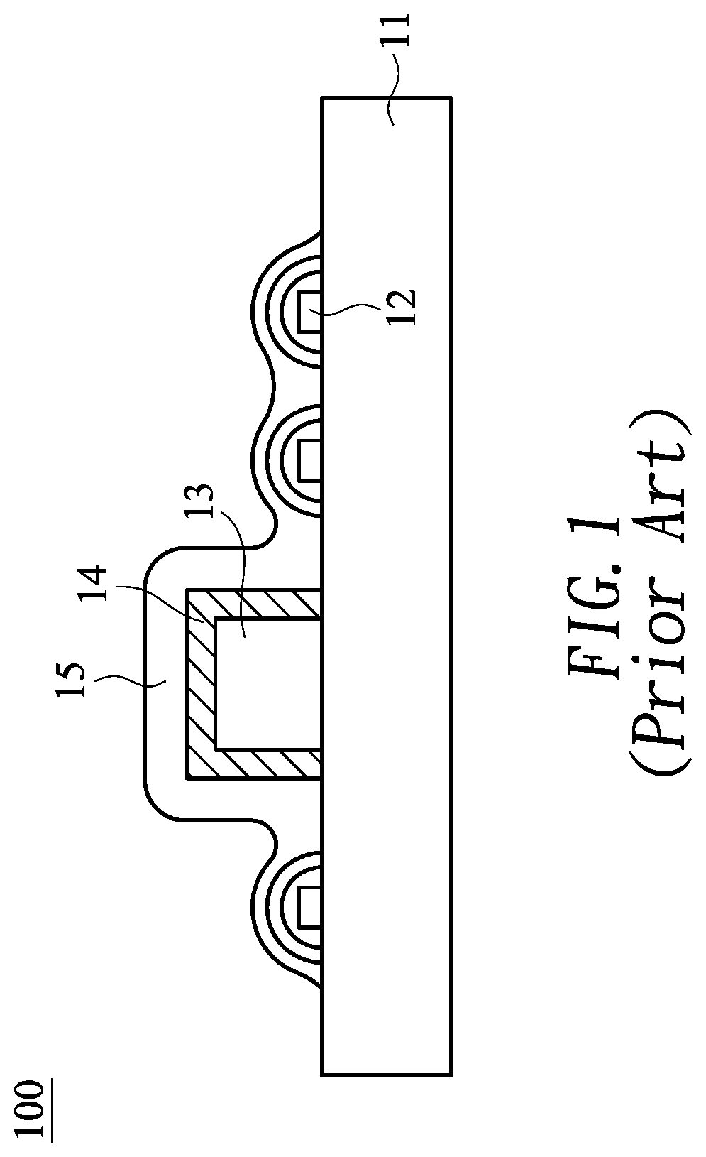
a technology of micro lightemitting diodes and micro led displays, which is applied in the direction of mechanical equipment, lighting and heating equipment, instruments, etc., can solve the problems of glass substrates b>11/b> and b>13/b> that may suffer damage, and achieve the effect of simplifying the process

Inactive Publication Date: 2020-07-30
PRILIT OPTRONICS INC
View PDF8 Cites 2 Cited by
  • Summary
  • Abstract
  • Description
  • Claims
  • Application Information

AI Technical Summary

Benefits of technology

The present invention provides a method for making a microLED display with a simplified process and a flat surface. The method involves steps of providing a substrate with microLEDs and an integrated circuit, forming a planarization layer to cover the microLEDs and the integrated circuit, which acts as both a light blocking layer and a corrosion-resistant layer.

Problems solved by technology

As a result, the glass substrate 11 may suffer fracture and / or the integrated circuit 13 may suffer damage.

Method used


Image

  • Microled display and a method of forming the same
  • Microled display and a method of forming the same
  • Microled display and a method of forming the same

Examples


Embodiment Construction

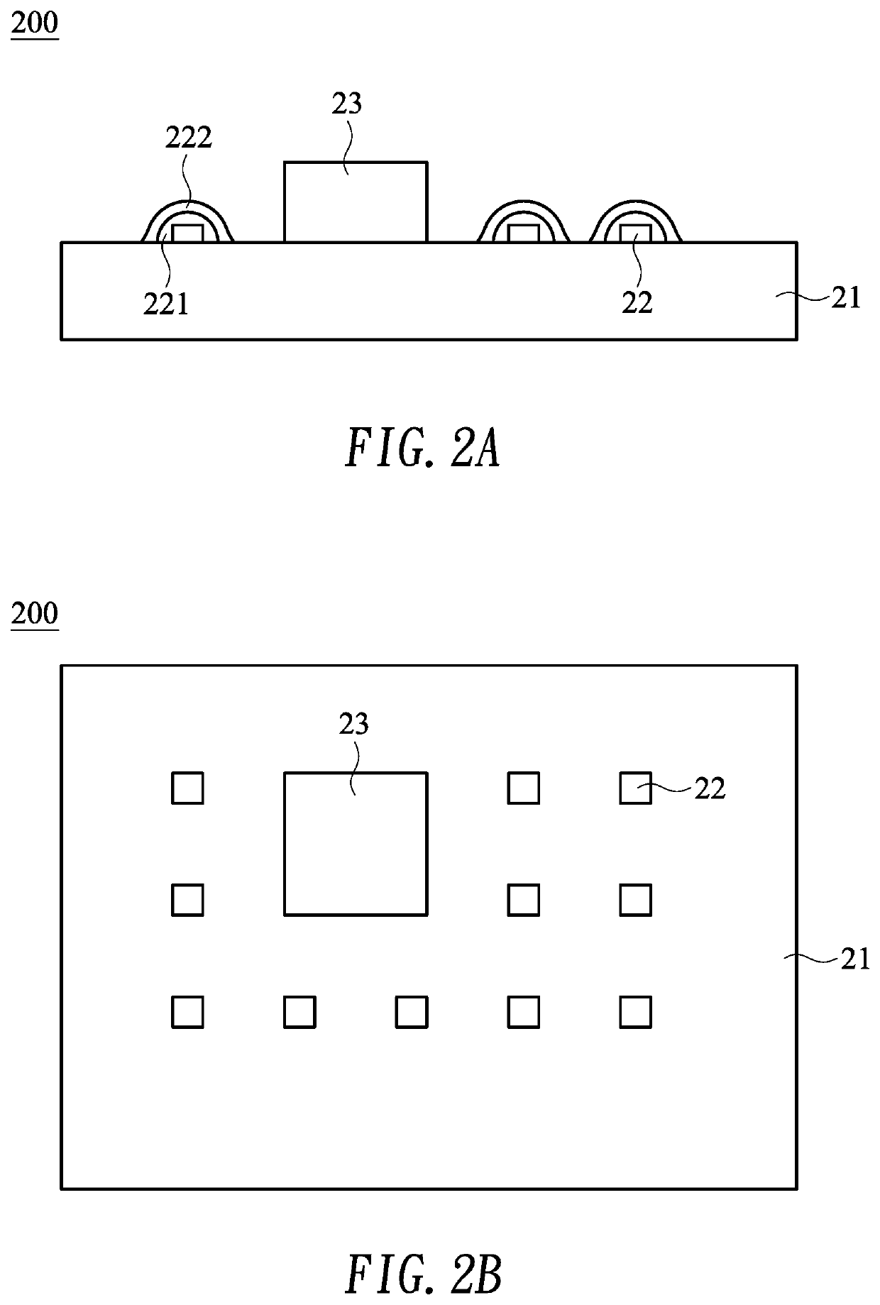
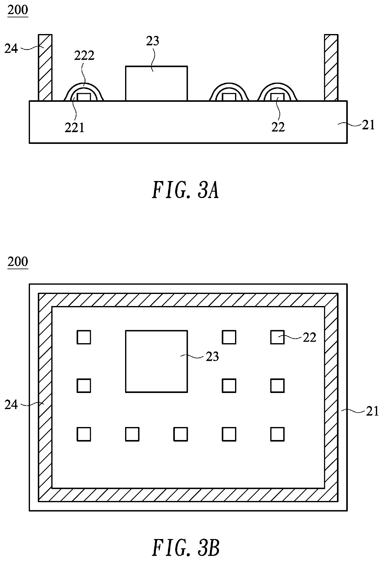
[0009]FIG. 2A to FIG. 4B show cross-sectional views and top views illustrating a method of forming a micro light-emitting diode (microLED or μLED) display 200 according to one embodiment of the present invention.

[0010]As shown in a cross-sectional view of FIG. 2A and an associated top view of FIG. 2B, a substrate 21 with microLEDs 22 and at least one integrated circuit 23 disposed thereon is provided. The substrate 21 may include glass or other materials suitable for supporting the microLEDs 22 and the integrated circuit 23. The integrated circuit 23 may, for example, be a driver that is mounted on the substrate 21 by chip-on-glass (COG) technique. It is appreciated that, although only a few microLEDs 22 are depicted, a large number of microLEDs 22 may commonly be disposed on the substrate 21. It is noted that, in the embodiment, the integrated circuit 23 has a height (e.g., 150 micrometers) being substantially larger than a height (e.g., less than 10 micrometers) of the microLED 22...


PUM

PropertyMeasurementUnit
sizeaaaaaaaaaa
heightaaaaaaaaaa
heightaaaaaaaaaa

Abstract

A method of forming a micro light-emitting diode (microLED) display includes providing a substrate with a plurality of microLEDs and at least one integrated circuit disposed thereon; and forming a planarization layer to cover the microLEDs and the at least one integrated circuit. The planarization layer acts as both a light blocking layer and a corrosion-resistant layer.

Description

BACKGROUND OF THE INVENTION1. Field of the Invention[0001]The present invention generally relates to a micro light-emitting diode (microLED), and more particularly to a method of forming a microLED display.2. Description of Related Art[0002]A micro light-emitting diode (microLED, mLED or μLED) display panel is one of flat display panels, and is composed of microscopic microLEDs each having a size of 1-10 micrometers. Compared to conventional liquid crystal display panels, the microLED display panels offer better contrast, response time and energy efficiency. Although both organic light-emitting diodes (OLEDs) and microLEDs possess good energy efficiency, the microLEDs, based on group III / V (e.g., GaN) LED technology, offer higher brightness, higher luminous efficacy and longer lifespan than the OLEDs.[0003]FIG. 1 shows a cross-sectional view of a conventional microLED display 100 with microLEDs 12 and an integrated circuit 13 disposed on a glass substrate 11. A first protective laye...

Claims


Application Information

Patent Timeline
Patent Type & Authority Applications(United States)
IPC IPC(8): H01L33/60H01L33/00H01L33/30F21V31/00F21V8/00
CPCH01L33/60G02B6/0073F21V31/005G02B6/0055H01L33/0062H01L33/30H01L25/167H01L33/58
Inventor LEE, HSING YINGWU, BIING-SENGCHUANG, SHIH-WEI
Owner PRILIT OPTRONICS INC
Why Eureka
Try Eureka