Display device and method of manufacturing display device

Inactive Publication Date: 2020-08-27
TRIVALE TECH
View PDF0 Cites 2 Cited by
  • Summary
  • Abstract
  • Description
  • Claims
  • Application Information

AI Technical Summary

Benefits of technology

The present invention aims to provide a display device that makes a pixel become a bright point defect inconspicuous when observed from within a viewing angle. It prevents the visual recognition of light emitted from the defective pixel region, making it difficult for a pixel adjacent to the defective pixel to be hidden. This results in a high-quality display. The invention does not require a significant increase of the light-blocking film, ensuring that the display device remains visually appealing.

Problems solved by technology

For manufacture of the display devices, as the numbers of pixels increase in the display devices, the ratio of display devices with pixels to become defects increases among the manufactured display devices.
Hence, the recent increase in the numbers of pixels of the display devices has inhibited improvement of manufacturing yield.
A pixel to become a defect is caused by failing to control the brightness level of light emitted from the pixel due to short-circuit of an electrode for controlling this brightness level, for example.
The pixel to become a bright point defect is conspicuous in a black background, easily recognizable, and reduces the visual quality of a display device.
As a result, the pixel defect can become inconspicuous (paragraph 0029).
According to the conventional techniques, however, a pixel to become a bright point defect is conspicuous in some cases when a display device is observed diagonally within a viewing angle.
This problem becomes serious, particularly in a display device having a wide viewing angle such as a liquid crystal display device with a liquid crystal display panel of a lateral field system.

Method used


Image

  • Display device and method of manufacturing display device
  • Display device and method of manufacturing display device
  • Display device and method of manufacturing display device

Examples


Embodiment Construction

1 Display Device in which Bright Point Defect is Repaired

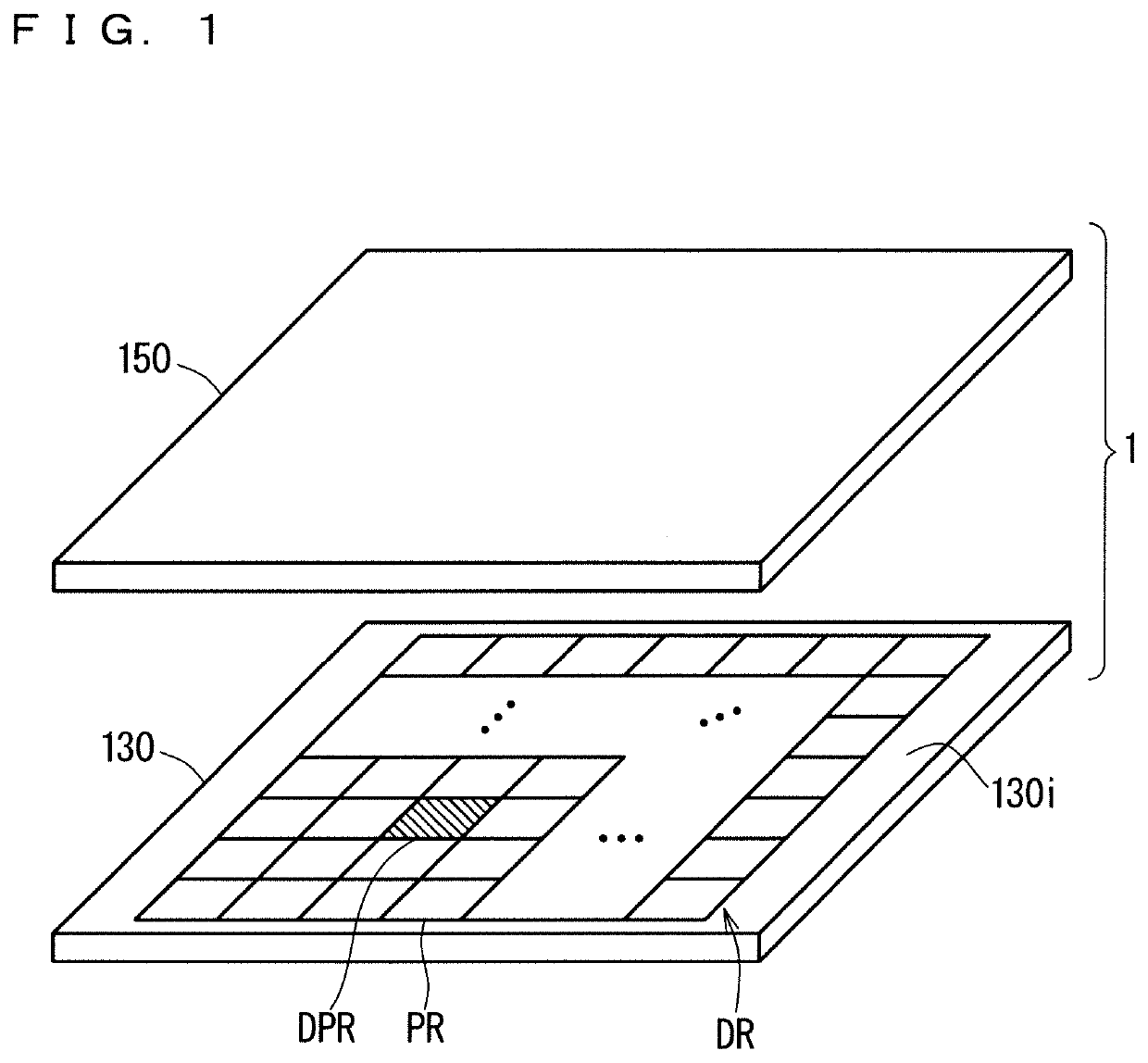
[0033]FIG. 1 is an exploded perspective view schematically illustrating a principal part of a display device in which a bright point defect is repaired in the same way as repair of a bright point defect in a liquid crystal display device of each of a first preferred embodiment and a second preferred embodiment.

[0034]A display device 1 shown in FIG. 1 includes a first substrate 130 and a second substrate 150. The display device 1 further includes a first layer and a second layer not illustrated.

[0035]The second substrate 150 faces the first substrate 130. The first substrate 130 has an internal main surface 130i. The internal main surface 130i is on the arrangement side of the second substrate 150. The internal main surface 130i includes a display region DR. The display region DR is partitioned into a plurality of pixel regions PR. The pixel regions PR are aligned regularly. A defective pixel region DPR is mixed in the pixel re...


PUM


Abstract

A display panel has a plurality of pixel regions to emit light. A second substrate faces a first substrate across a display medium layer, is transparent, includes a part having a thickness of less than 0.3 mm, and has a main surface on the opposite side to the arrangement side of the first substrate. A light-blocking film is arranged on the main surface and on the part, and overlaps a defective pixel region and projects from the defective pixel region by a width W in a plan view taken from the thickness direction of the display panel. The width W is equal to or more than a width W1 that prevents visual recognition of light emitted from the defective pixel region when the display panel is observed from within a viewing angle.

Description

FIELD OF THE INVENTION[0001]The present invention relates to a display device and a method of manufacturing the display device.BACKGROUND ART[0002]A display device includes a plurality of pixels. In each of the pixels, the brightness level of a light beam emitted from each pixel is controlled. By doing so, an image responsive to the brightness levels of light beams emitted from the pixels is displayed on the display device.[0003]In response to size increase and higher resolution of display devices in recent years, the number of pixels of the display devices is on the increase. For manufacture of the display devices, as the numbers of pixels increase in the display devices, the ratio of display devices with pixels to become defects increases among the manufactured display devices. Hence, the recent increase in the numbers of pixels of the display devices has inhibited improvement of manufacturing yield.[0004]A pixel to become a defect is caused by failing to control the brightness le...

Claims


Application Information

Patent Timeline
IPC IPC(8): G02F1/1335G02F1/135G02F1/1333
CPCG02F1/133512G02F1/133305G02F1/135G02F2001/1351G02F1/1309G02F1/136259G02F2201/506G02F1/1351
Inventor HIGASHI, TAKUYA
Owner TRIVALE TECH
Why Eureka
Try Eureka