Supercharge Your Innovation With Domain-Expert AI Agents!

Expediting Spectral Measurement in Semiconductor Device Fabrication

a semiconductor device and spectral measurement technology, applied in the direction of semiconductor/solid-state device testing/measurement, optical radiation measurement, instruments, etc., can solve the problems of reducing process efficiency and increasing overall processing tim

Active Publication Date: 2020-12-17
KLA CORP
View PDF0 Cites 2 Cited by
  • Summary
  • Abstract
  • Description
  • Claims
  • Application Information

AI Technical Summary

Benefits of technology

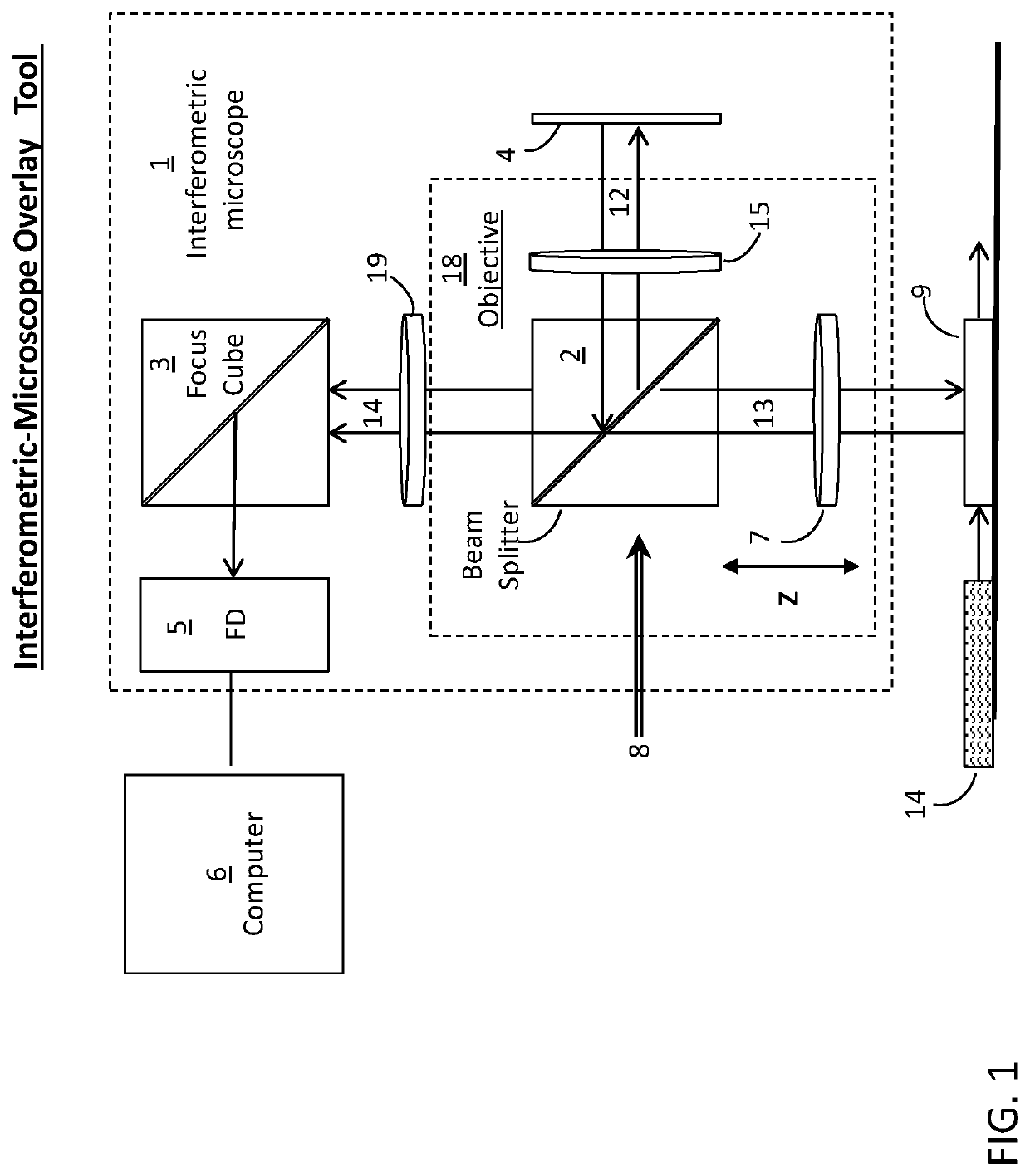
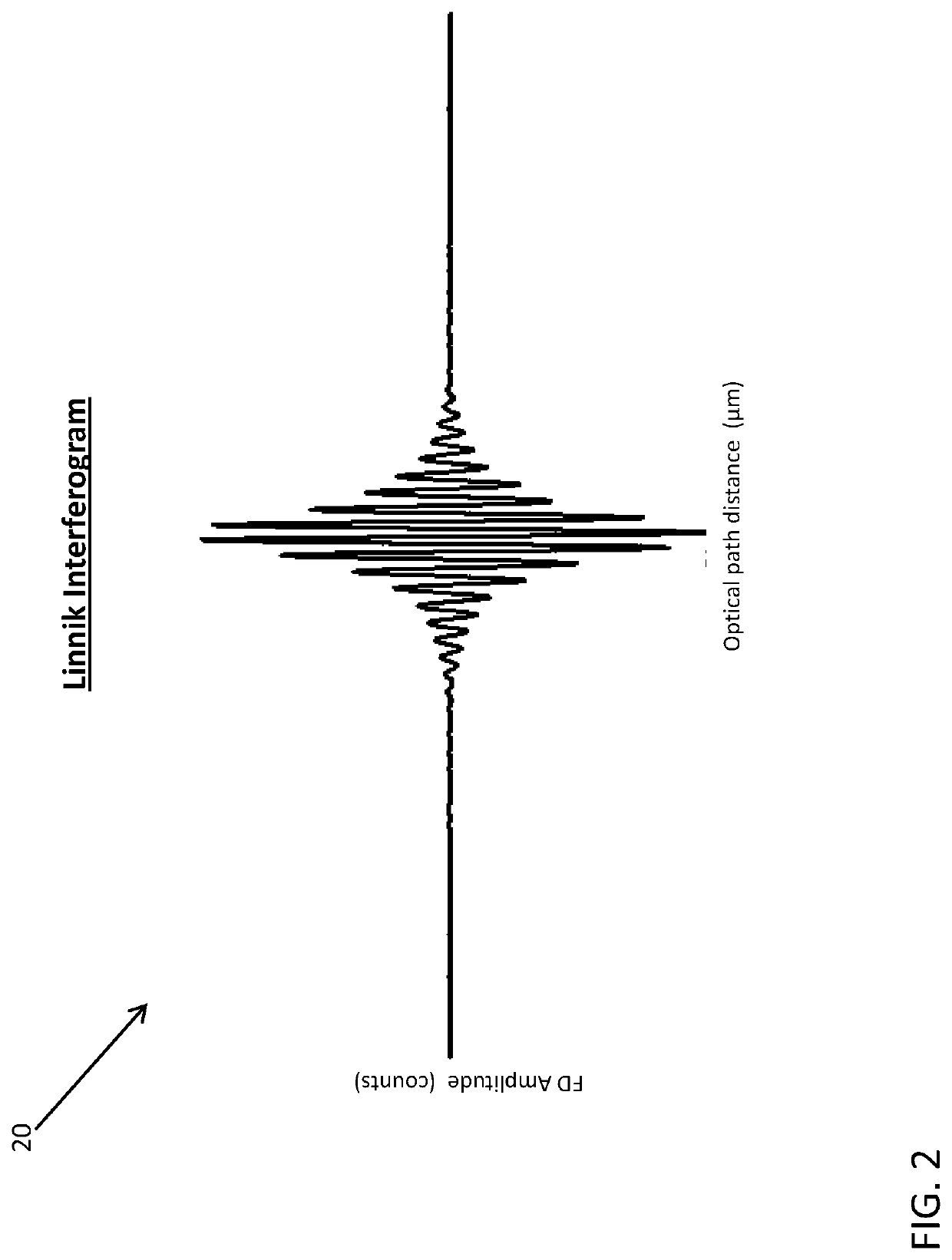
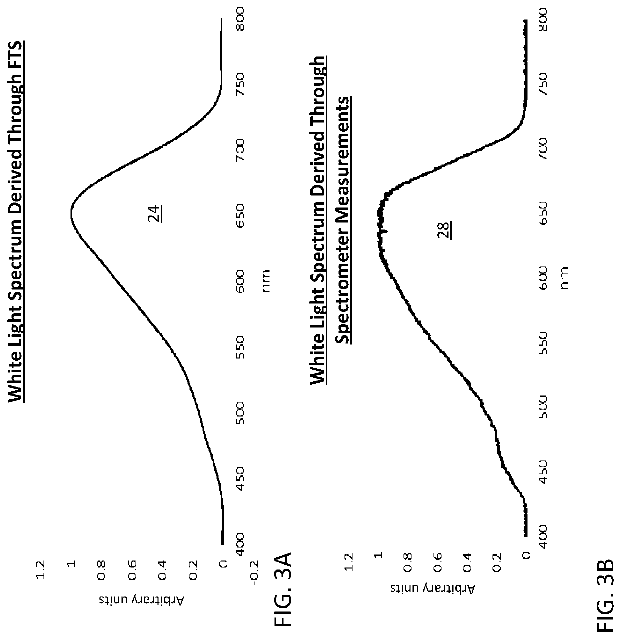
The present invention provides an interferometric-spectroscopy metrology tool that can capture and analyze the spectrum of white light illumination during vertical conveyance of a focal lens using an interferometric microscope. The tool includes an interferometer and a computer that applies a Fourier transformation to the interferogram to render it into a frequency spectrum. The tool can also capture the spectral reflectivity of the processed wafer in the interferogram and analyze it to determine the spectral reflectivity of the wafer. The invention also provides a method for expediting the acquisition of hyperspectral data in semiconductor device fabrication metrology.

Problems solved by technology

Spectral measurements many times increase overall processing time thereby reducing process efficiency.

Method used


Image

  • Expediting Spectral Measurement in Semiconductor Device Fabrication
  • Expediting Spectral Measurement in Semiconductor Device Fabrication
  • Expediting Spectral Measurement in Semiconductor Device Fabrication

Examples


Embodiment Construction

[0037]In the following description, numerous details are set forth to facilitate a clear understanding of the invention and it should be appreciated that the present invention may be practiced without these specific details. Furthermore, well-known methods, components and procedures are omitted to highlight the present invention.

[0038]The following terminology will be used through this document:

[0039]“Metrological activities” includes and not limited to any one or combination metrological tests:

[0040]“Overlay metrology” (OVL) refers to a technique for evaluating alignment between upper and lower layer patterns most effectively evaluated at certain wavelengths.

[0041]The OVL variance is calculated as the difference between centers of symmetry of inner and outer overlay targets.

[0042]“Kernel3S” refers to a metric that is three times the variance of the OVL calculated by three different overlying parts of the same overlay targets. It should be as small as possible while high values may ...


PUM

PropertyMeasurementUnit
frequency spectrumaaaaaaaaaa
illuminationaaaaaaaaaa
spectral reflectivityaaaaaaaaaa

Abstract

A device and method for expediting spectral measurement in metrological activities during semiconductor device fabrication through interferometric spectroscopy of white light illumination during calibration, overlay, and recipe creation.

Description

CROSS-REFERENCE TO RELATED APPLICATIONS[0001]This application is a divisional of U.S. application Ser. No. 15 / 568,958 filed Oct. 24, 2017, which is a national stage application of PCT / US2017 / 048276 filed Aug. 23, 2017, which claims priority to U.S. App. No. 62 / 403,712 filed Oct. 4, 2016, the disclosures of which are hereby incorporated by reference.BACKGROUND OF THE INVENTION[0002]Typically, spectral information used in metrological activities associated with semiconductor device manufacture is acquired through relatively time consuming spectral measurements during calibration, overlay activities, recipe creation, and other metrological activities. Spectral measurements many times increase overall processing time thereby reducing process efficiency. Therefore, there is a need to expedient acquisition of robust spectral information enabling a wide range of metrological activities in a manner preserving fabrication speed and efficiency.SUMMARY OF THE INVENTION[0003]According to the te...

Claims


Application Information

Patent Timeline
Patent Type & Authority Applications(United States)
IPC IPC(8): G01N21/45G01B11/06G01N21/55
CPCG01N2201/0633G01N2201/066G01N2201/0636G01B11/0675G01N21/45G01N21/55G01N21/31G01N21/956G03F7/70633G02B21/0056G02B21/082G02B21/365H01L22/12G03F7/706837G03F7/706849G03F7/70653G02B21/0016G01J3/453G01N21/9501G02B21/06G02B21/18H01L21/67259
Inventor IMMER, VINCENTMARCIANO, TALLAVERT, ETAY
Owner KLA CORP
Features
  • R&D
  • Intellectual Property
  • Life Sciences
  • Materials
  • Tech Scout
  • Unparalleled Data Quality
  • Higher Quality Content
  • 60% Fewer Hallucinations
Learn More