Pixel array of a thermal pattern sensor, sensor associates with coil heating lines
a thermal pattern sensor and pixel array technology, applied in the field of thermal pattern sensors, can solve the problems of increasing the manufacturing cost of the sensor, reducing the efficiency of the sensor production, and limited space available on the support s, so as to facilitate the signal routing
- Summary
- Abstract
- Description
- Claims
- Application Information
AI Technical Summary
Benefits of technology
Problems solved by technology
Method used
Image

Examples
Embodiment Construction
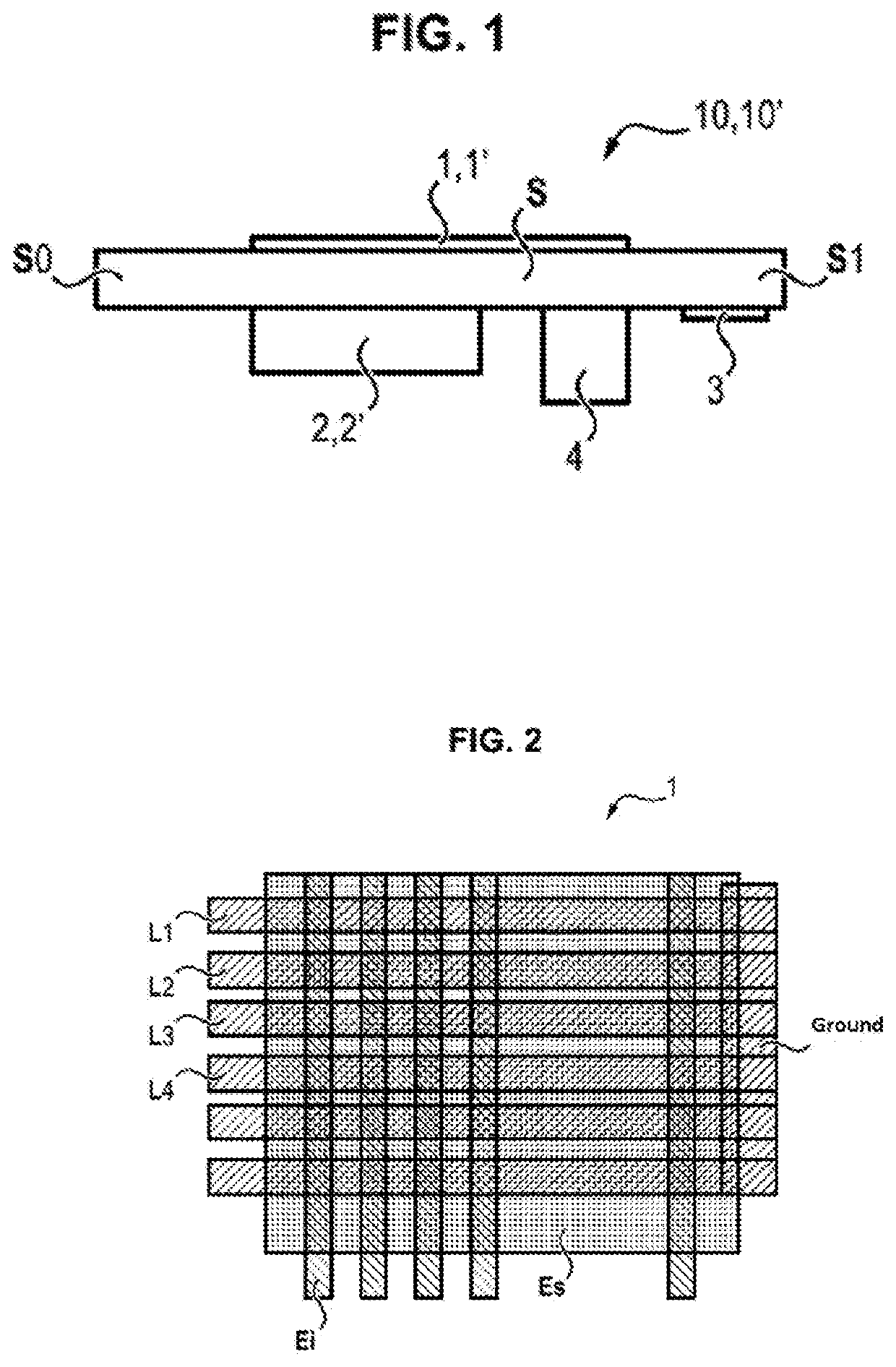
[0038]A sensor according to the invention has the same structure as that in the introduction and comprises a support S comprising a lower surface S0 and an upper surface S1. Such a support S is for example a substrate made of PET or PEN or PI or else of CIU type (ABF, FR4) or else made of glass.
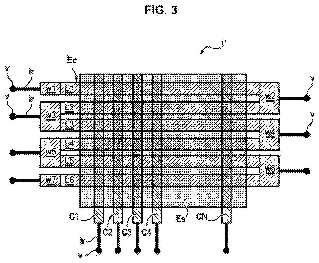
[0039]On the upper surface Si is disposed a sensitive element 1′, a top view of which is illustrated in FIG. 3 and is constituted by a pixel matrix comprising several rows and several columns of pixels.
[0040]On the lower surface S0 are disposed an integrated circuit 2′ such as an ASIC, an element 4 (optional) and where applicable contacts 3 making it possible to connect the sensor to the contacts of a chip card when such a sensor is disposed on such a card. Of course, it can be connected to other systems (telephone, access control terminal etc.)
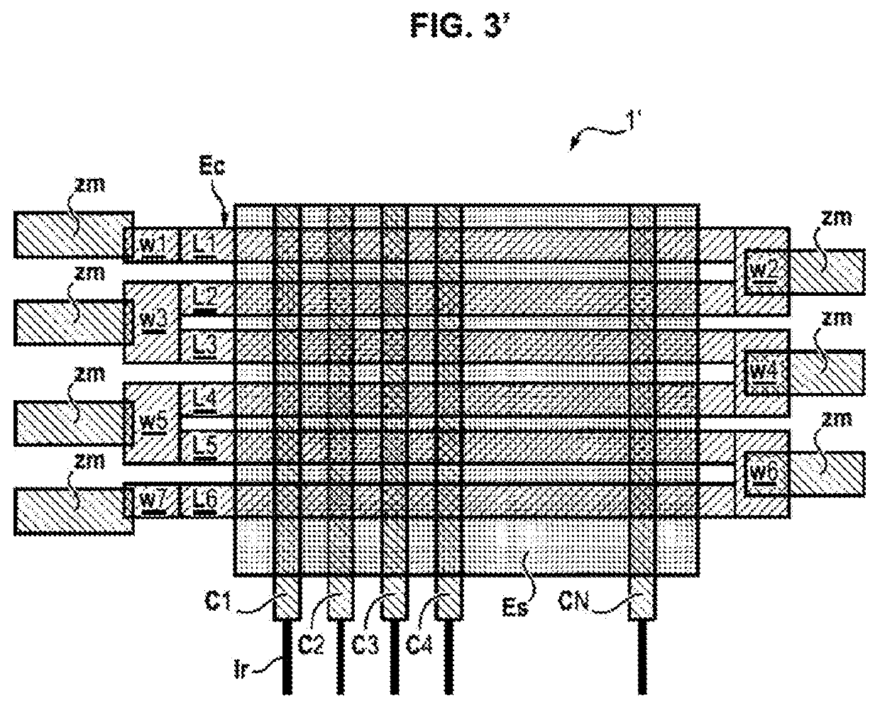
[0041]The invention described here notably aims to replace the pixel matrix 1 of FIGS. 1 and 2 with the pixel matrix 1′ which will be described below,...
PUM
 Abstract
- an active thermal element formed by a thermosensitive material disposed between a lower layer and an upper layer, the lower layer being constituted by a plurality of first tracks made of electrically conductive material and extending along a first direction, said first tracks forming pixel columns;
- a heating element, disposed on the active thermal element and forming a serpentine path, said heating element being constituted by a plurality of second tracks (L1, L2, L3, L4, L5, L6) made of electrically conductive material and connecting segments (w1, w2, w3, w4, w5, w6) made of electrically conductive material connected to the ends of the second tracks (L1, L2, L3, L4, L5, L6), said second tracks (L1, L2, L3, L4, L5, L6) extending in a second direction different from the first direction and forming lines of pixels, the second tracks being connected except for the first and last second tracks (L1, L2, L3, L4, L5, L6), by their respective ends to one of the ends of a second preceding track and a second following track by way of said connecting segments (w1, w2, w3, w4, w5, w6), the first and last second tracks each having a free end connected to a connecting segment.
Description
Claims
Application Information
 - R&D Engineer
- R&D Manager
- IP Professional
- Industry Leading Data Capabilities
- Powerful AI technology
- Patent DNA Extraction
Browse by: Latest US Patents, China's latest patents, Technical Efficacy Thesaurus, Application Domain, Technology Topic.
© 2024 PatSnap. All rights reserved.Legal|Privacy policy|Modern Slavery Act Transparency Statement|Sitemap