
Gate driving unit and gate driving method

Active Publication Date: 2021-02-25
SHENZHEN CHINA STAR OPTOELECTRONICS SEMICON DISPLAY TECH CO LTD
View PDF0 Cites 0 Cited by
  • Summary
  • Abstract
  • Description
  • Claims
  • Application Information

AI Technical Summary

Benefits of technology

The present patent provides a gate driving unit and method that includes a reset unit and a pull-down control unit. The reset unit includes a reset transistor that pulls down the drain of a first transistor when an external control signal is at a high level. The pull-down control unit includes an eighth and a ninth transistor that pull down the drain of the first transistor when a second clock signal is at a high level. The technical effect of this patent is to provide a more efficient and reliable gate driving unit and method for driving a circuit.

Problems solved by technology

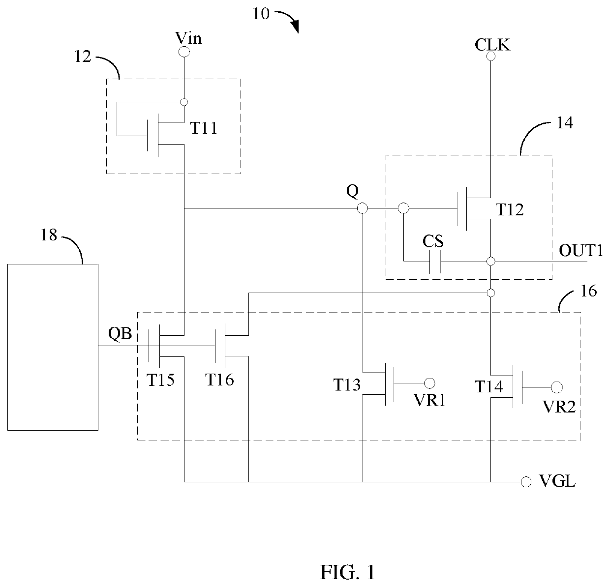
However, manufacturing technology of forming a channel of TFTs by using metal oxide is immature, often leading to a negative threshold voltage of the TFTs and turning the TFTs into depletion-type TFTs that continuously consume energy.
When receiving a negative pressure under illumination, the threshold voltage drift to negative, so electrical leakage and increased power consumption caused by the negative threshold voltage during circuit design needs to be considered.
At the same time, due to the negative threshold voltage of the TFT, the high electric level outputted by the output terminal (ie, QB node) of the pull-down control circuit 18 shown in FIG. 1 cannot reach an expected high electric level, causing an overly slow speed of pull-down in the pull-down phase, as well as a problem of unstable electric level in the electric level maintaining phase, affecting the function of the gate driving unit 10.
However, this implementation leads to a substantial increase in the number of transistors required, resulting in increased manufacturing cost while being disadvantageous to the making of lightweight and thin display panels.

Method used


Image

  • Gate driving unit and gate driving method
  • Gate driving unit and gate driving method
  • Gate driving unit and gate driving method

Examples


Embodiment Construction

[0045]The gate driving circuit and the gate driving method provided by the embodiments of the present invention are described in detail below with reference to the accompanying figures. It is obvious that the described embodiments are only part of the embodiments of the present disclosure, and not all of the embodiments. All other embodiments obtained by those skilled in the art based on the embodiments of the present disclosure without inventive steps are within the scope of the present disclosure.

[0046]FIG. 4 shows a circuit diagram of a gate driving circuit of the present disclosure. The gate driving circuit 40 consists of N+1 gate driving units 42. FIG. 5 shows a circuit diagram of a gate driving unit 42 of a first embodiment of the present disclosure. Please referring to FIG. 4 and FIG. 5 together, the gate driving unit 42 has an input unit 50, a driving unit 52, a pull-down unit 54, a pull-down control unit 56, and a reset unit 58.

[0047]The input unit 50 includes a first trans...


PUM


Abstract

A gate driving unit and a gate driving method are provided. The gate driving unit includes an input unit, a driving unit, a pull-down unit, and a pull-down control unit. The pull-down unit has an output terminal of a current stage cascaded signal and an output terminal; in the pull-up phase, the output terminal of the current stage cascaded signal and the output terminal output signal, a voltage of the output terminal of the current stage cascaded signal is pulled down to a first reference low electric level, and a voltage of the output terminal is pulled down to a second reference low electric level.

Description

FIELD OF INVENTION[0001]The present disclosure relates to the field of display technologies, and more particularly, to a gate driving unit and a gate driving method.BACKGROUND OF INVENTION[0002]With the advancement of display technology, display quality of display devices has been improved. In order to provide users a better visual experience, frames of display devices are gradually narrowing and developing towards frameless.[0003]The technology of integrating thin film transistors (TFT) by gate on array (GOA), that is, integrating a GOA unit into an array substrate that includes TFTs arranged in an array, which replaces a conventional arrangement that gate drive units and source drive units are disposed on a longitudinal side and a lateral side of the display panel, can reduce a number of wafers disposed outside the display area. At the same time, the integrated arrangement of a driver module can simplify a packaging process and reduce a space required by the driver module to facil...

Claims


Application Information

Patent Timeline
IPC IPC(8): G11C19/28G09G3/20
CPCG11C19/28G09G2310/0267G09G2310/08G09G3/20G09G3/3266G09G3/3677G09G2310/0286G11C19/287
Inventor ZHANG, SHENGDONGLIAO, CONGWEIHAN, BAIXIANGXUE, YANZHANG, LIUQI
Owner SHENZHEN CHINA STAR OPTOELECTRONICS SEMICON DISPLAY TECH CO LTD
Learn More