See-through display for an augmented reality system

Pending Publication Date: 2021-06-17
TECH INNOVATION MOMENTUM FUND ISRAEL
View PDF0 Cites 2 Cited by
  • Summary
  • Abstract
  • Description
  • Claims
  • Application Information

AI Technical Summary

Benefits of technology

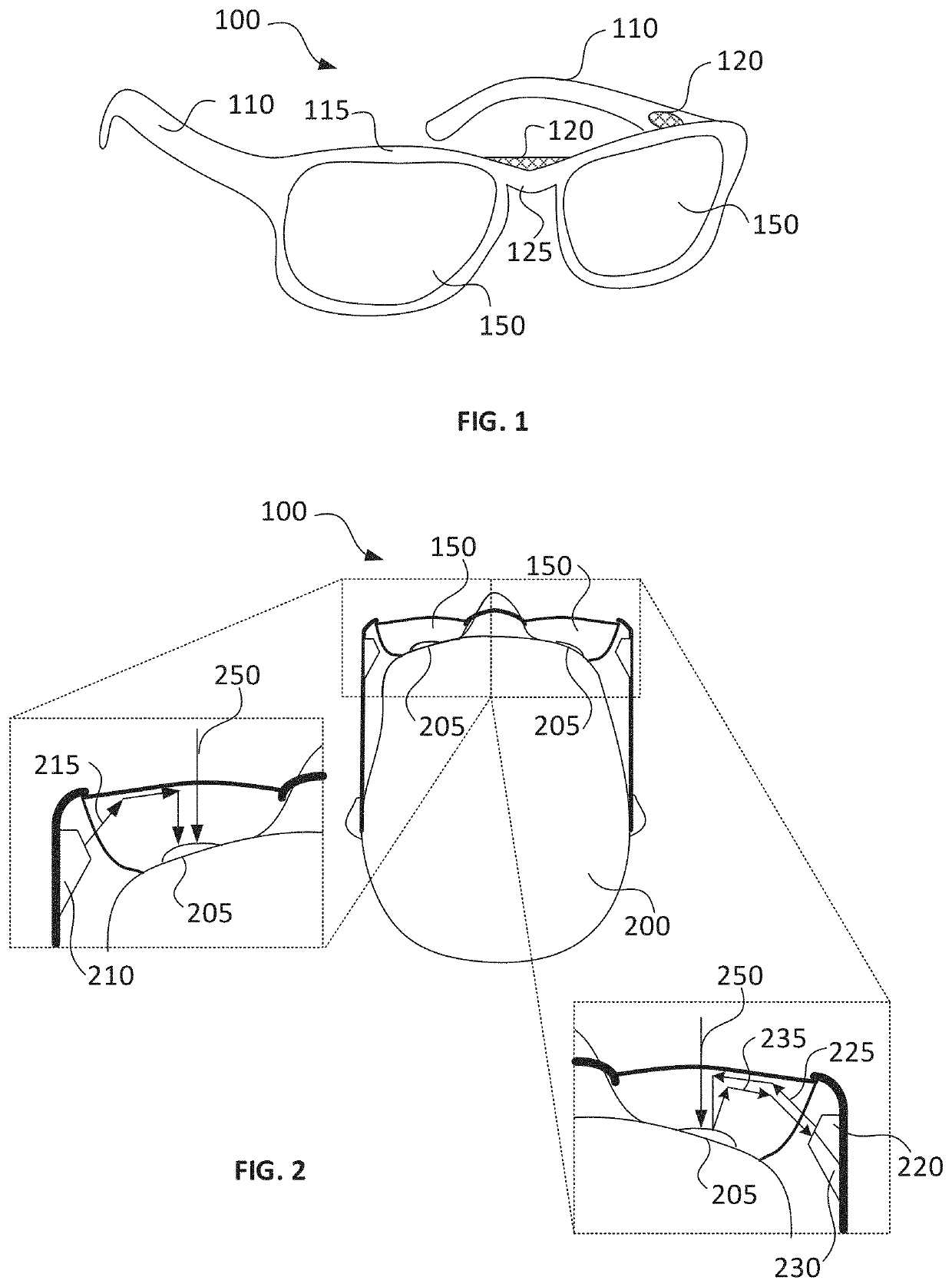
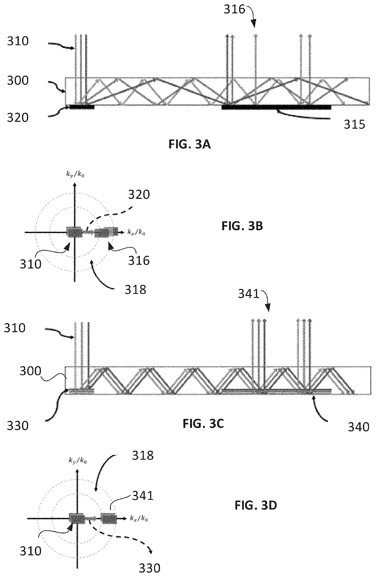
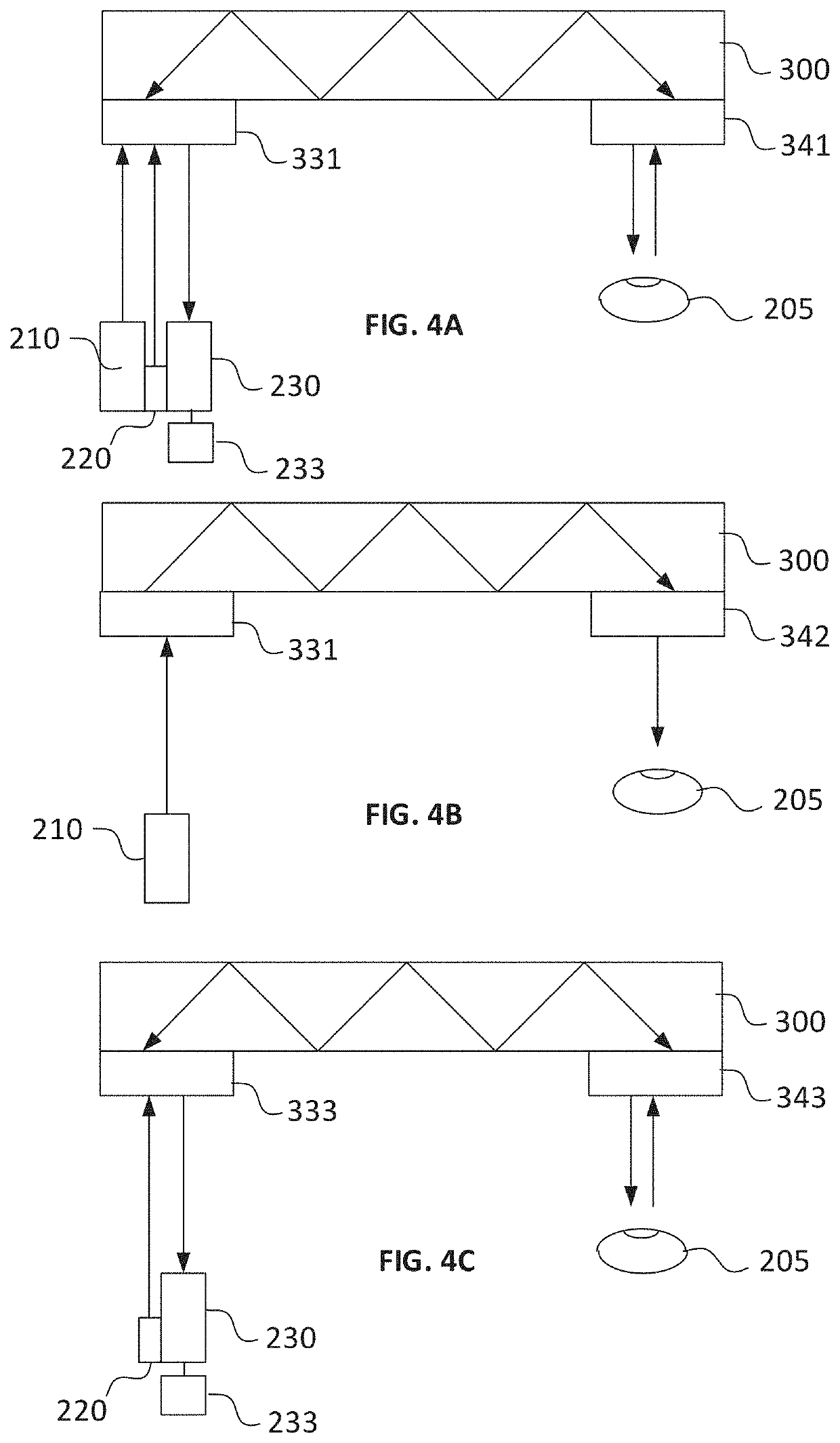
[0006]According to an aspect of some embodiments, there is provided a display that is see-through, has a favorable form factor and improved chromatic behavior. A see-through display as defined herein is a display that is at least partially transparent to light in the visible range to visible light. In some example embodiments, the see-through display is a near-eye visor for an augmented reality system. According to some example embodiments, the see-through display includes a visibly transparent stack of MS layers configured to couple a relatively broadband signal in and out of a single waveguide (WG). The ability to use a single WG provides for reducing width of the display. Each layer in the MS stack may act as provide a resonant response at a defined spectral band

Problems solved by technology

The chromatic aberrations of DOEs and (HOEs) however, are large, and therefore not suited for a broadband spectrum of visual light.

Method used


Image

  • See-through display for an augmented reality system
  • See-through display for an augmented reality system
  • See-through display for an augmented reality system

Examples


example 1

[0097]FIGS. 9A and 9B show an example single silver disc simulation scheme and transmission of the example single silver disc for several disc radii respectively, both in accordance with some example embodiments. FIGS. 9C and 9D show an example three layer of metallic discs simulation scheme and transmission of Al, Ag and Au disc stack design for 450 nm, 550 nm and 650 nm respectively, both in accordance with some example embodiments. A commercially available optical simulations software (Lumerical FDTD available by Lumerical in Canada) was applied to simulate the spectral properties of the different layers composing the MS. FIG. 9A shows an FDTD simulation scheme of a single nano size silver particle. In FIG. 9B, the transmission spectra of this particle is shown for several radii. It was found that the resonance's center wavelength was red-shifted as the particle radius is increased. In some example embodiments, such a dependence may be utilized to design a stack of three differen...

example 2

[0098]FIG. 10A shows a scanning electron microscope image of a sample gold MS. FIG. 10B shows a zoomed-in section of the sample. A periodic nature of the sample, composed of arrays of gold nanodiscs is clearly visible. It is seen that the nanodiscs are relatively uniform. The measured diameter was 140 nm±4 nm, with inter-particle spacing of 180 nm±8 nm. Improved performance may be achieved by altering particle size and inter-particle spacing. Optionally, a duty cycle of a periodic function of the sample may also be altered to widen the nanodiscs zone's width.

example 3

[0099]FIG. 11A shows a scanning electron microscope image of an aluminum MS. The MS is a single MS binary plasmonic MS, designed to manipulate red light. The nano-structures sizes are 130±5 nm with an inter-particle spacing of 200 nm. FIG. 11B shows a zoomed-in section of the MS. The MS was fabricated using e-beam lithography (Raith e-Line). An indium-tin-oxide covered glass was used as the substrate. After the e-beam process, 40 nm thick Aluminum film was then deposited by e-beam evaporation and subsequently lifted off.


PUM


Abstract

An optical system for a see-through display includes a stack of metasurface layers configured to receive light constituting an image; and a waveguide coupled to the stack. Each layer in the stack of metasurface layers is configured to provide a resonant response to an optical field at a different spectral band and to couple the resonant response with a waveguide. The waveguide is configured to propagate the different spectral bands in a direction of a user's eye.

Description

FIELD AND BACKGROUND OF THE INVENTION[0001]The present invention, in some embodiments thereof, relates to a see-through display and, more particularly, but not exclusively, to a near-eye visor. In preferred embodiments, the near-eye visor serves as a display of an augmented reality system.[0002]Near-eye visors for augmented reality systems are typically transparent to visible light. Form factor of near-eye visors is a parameter in promoting widespread acceptance of augmented reality systems at least for consumer electronics applications. Attempts have been made to replace some bulk optics, e.g. free-form optics, with more compact and lightweight elements. Example elements include diffractive optical elements (DOEs) or holographic optical elements (HOEs) designed to couple light in and out of a waveguide (WG) in transmission or reflection mode. The chromatic aberrations of DOEs and (HOEs) however, are large, and therefore not suited for a broadband spectrum of visual light. One solut...

Claims


Application Information

Patent Timeline
IPC IPC(8): G02B27/01G06F3/01H04N5/225G02B1/00F21V8/00
CPCG02B27/0172G06F3/013H04N5/2253H04N5/2256G02B27/0179G02B2027/0118G02B6/005G02B2027/0187G02B2027/0138G02B2027/014G02B1/002A61B3/113G02B2027/0112G02B2027/0178H04N23/54H04N23/56
Inventor ELLENBOGEN, TALAVAYU, ORIDITCOVSKI, RAN
Owner TECH INNOVATION MOMENTUM FUND ISRAEL
Why Eureka
Try Eureka