

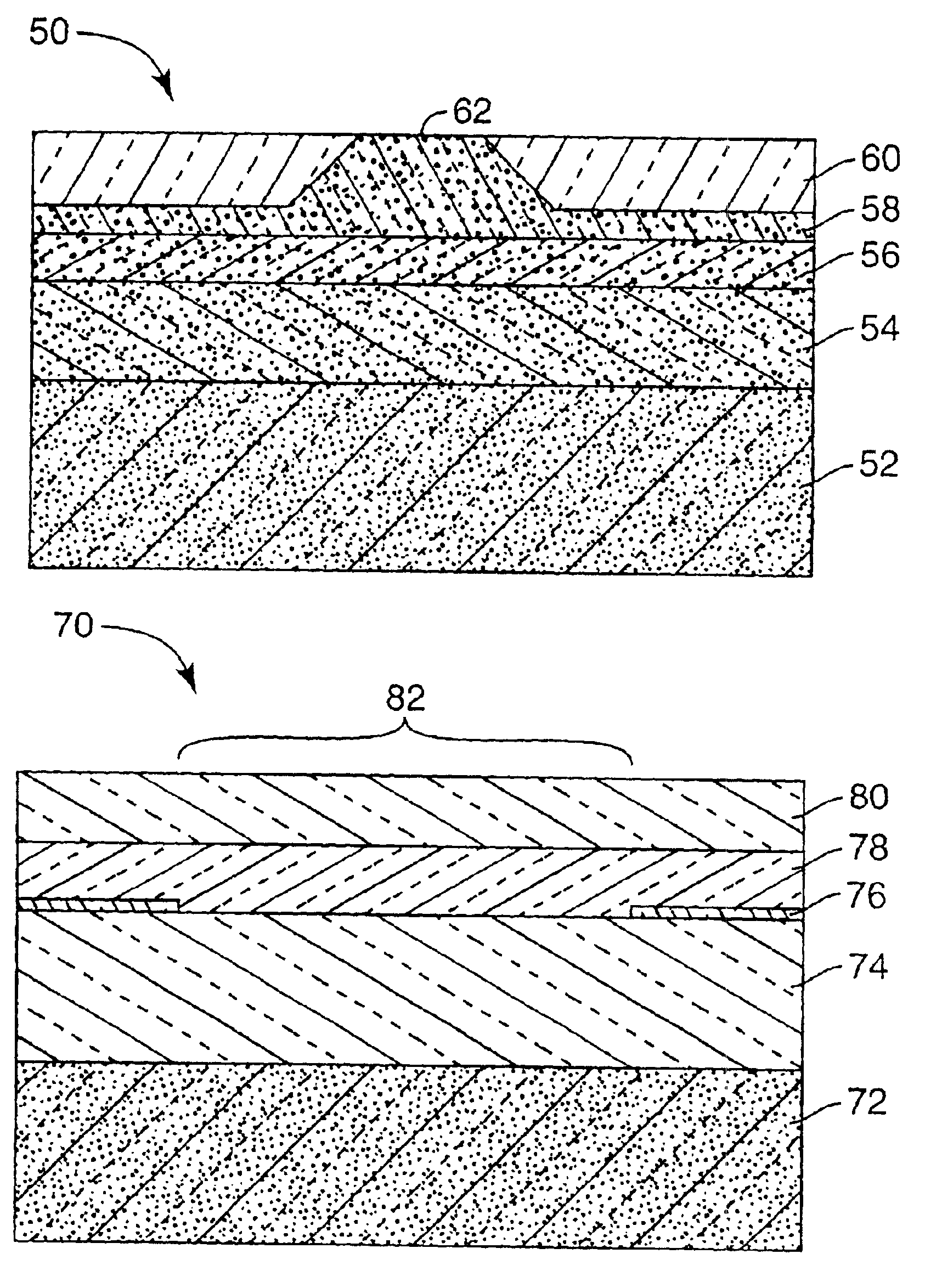
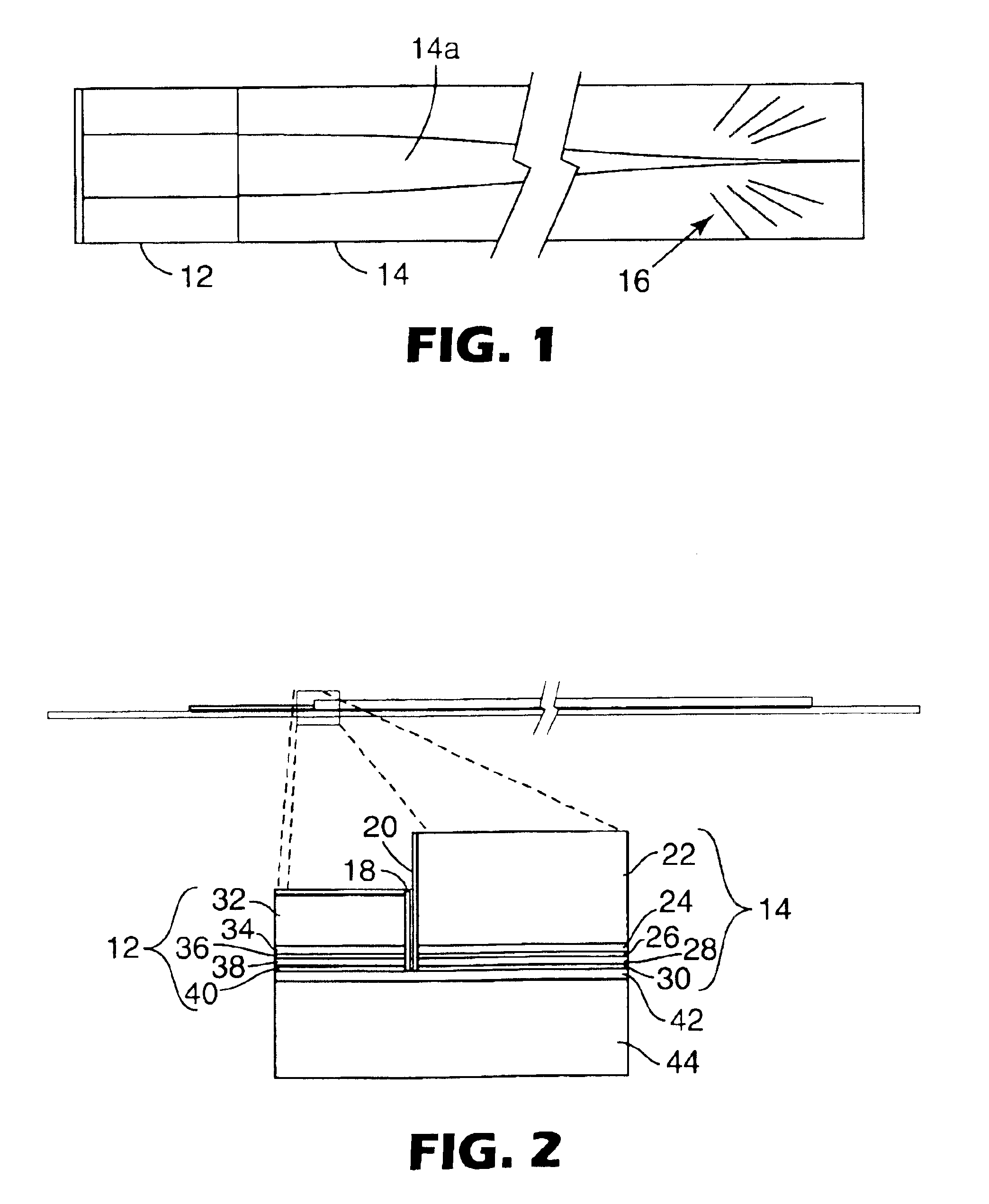
Laser diode chip with waveguide
a laser diode and waveguide technology, applied in the field of waveguides, can solve the problems of limiting the single-transverse mode laser diode, difficult to focus into a small area such as the end of an optical fiber, and high power density at the aperture, so as to achieve high output power and high optical damage threshold. , the effect of high power density
- Summary
- Abstract
- Description
- Claims
- Application Information
AI Technical Summary
Benefits of technology
Problems solved by technology
Method used
Image

Examples
example 1
980 nm Laser
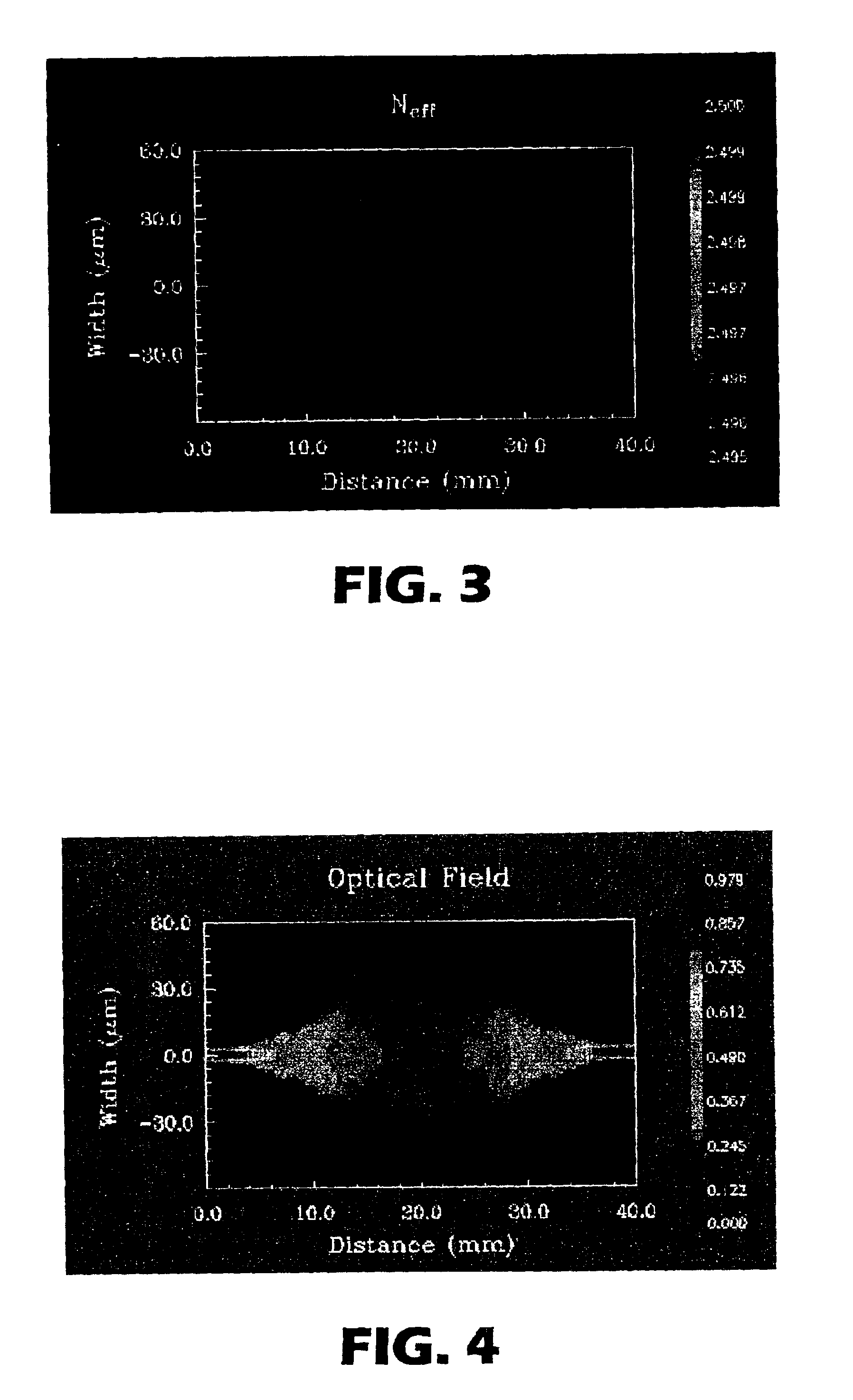
This example describes a 980 nm laser including an AlGaAs—GaInAs laser diode chip, a BeZnSe—BeZnTe tapered waveguide, and a silicon submount.
AlGaAs—GaInAs Laser Diode Chip
In this example a laser diode chip is grown by molecular beam epitaxy (MBE) on a (100) GaAs:Si semiconductor wafer. The lower cladding is AlxGa1-xAs:Si (x=0.2, n=1017 cm−3), 1 μm thick. The active region (laser waveguide core) is 1 μm thick undoped GaAs with three GayIn1-yAs quantum wells (y=0.8) in its center. The wells are separated from each other by 20 nm of GaAs. The thickness (growth time) of the quantum wells are adjusted to provide the desired laser wavelength (980 nm), and are approximately 7 nm. The upper cladding is AlxGa1-xAs:Be (x=0.2, p=1017 cm−3), 1 μm thick. The contact layer is GaAs:Be (p=1019 cm−3, 50 nm thick).
Fabrication of the laser diode chip begins with deposition of the p-ohmic contact metal, consisting of 20 nm Pd, 100 nm Au and 2 nm Ti, on the contact layer. The Ti facilitates ...
example 2
1480 nm Laser
This example describes a 1480 nm laser including an AlGaInAs—InP laser diode chip, a silicon oxynitride tapered waveguide chip, and a silicon submount.
AlGaInAs—InP Laser Diode Chip
In this example the laser diode wafer is grown by metal organic chemical vapor deposition (MOCVD) on a (100) InP:S wafer. All layers are nominally lattice-matched to the Inp. The lower cladding is InP:S (n=1018 cm−3), 0.8 μm thick, plus 0.1 μm of AlGaInAs:S (Eg=1.44 eV, n=1018 cm−3). The active region (laser waveguide core) is 0.28 μm thick undoped AlGaInAs (Eg=1.1 eV) with five GaInAs quantum wells at its center. The wells are separated from each other by 10 nm of AlGaInAs (Eg=1.1 eV). The thickness (growth time) of each of the quantum wells is adjusted to provide the desired laser wavelength (1480 nm). The upper cladding includes 0.1 μm of AlGaInAs:Zn (Eg=1.44 eV, p=1018 cm−3) and 1.3 μm of InP:Zn (p=1018 cm−3). The p-ohmic contact layers are 0.05 μm of GaInAsP (Eg=0.95 eV, p=2×1018 cm−3) an...
PUM
 Abstract
Description
Claims
Application Information