Compact polarization-insensitive optical receiver

a polarization-insensitive, optical receiver technology, applied in the direction of optical elements, instruments, optical waveguide light guides, etc., can solve the problems of complex polarization multiplexing at the transmitter and receiver sides, complicated realization of polarization-insensitive devices, and limited commercial interest, so as to mitigate undetectable discrepancies

Active Publication Date: 2013-07-25
CIENA
View PDF4 Cites 36 Cited by
  • Summary
  • Abstract
  • Description
  • Claims
  • Application Information

AI Technical Summary

Benefits of technology

[0017]Also advantageously, embodiments according to this aspect of the invention allow mitigating undesired discrepancies between the optical paths associated with the two substantially orthogonal polarization components such as fabrication inaccuracies, material non-uniformities and thermal fluctuations by arranging the delay lines of the first and second interferometric modules into spiraling structures and by intertwining these spiraling structures with each other.

Problems solved by technology

Indeed, as data transfer rates rise toward 100 Gb / s, coherent communication involving polarization multiplexing further adds to the complexity at the transmitter and receiver sides.
However, submicron SOI circuits generally support the propagation of only one polarization mode, typically a transverse electric (TE) mode, thereby complicating the realization of polarization-insensitive devices, which is highly desirable for telecommunication receivers.
Single-polarization optical receivers based on submicron SOI circuits have been reported [see, e.g., S. Faralli et al., “25 Gbaud DQPSK Receiver Integrated on the Hybrid Silicon Platform”, IEEE International Conference on Group IV Photonics (GFP), paper FA4 (2011)], but their commercial interest is limited.
However, in addition to sacrificing the high compactness provided by submicron waveguides, polarization-insensitivity remains a challenge as both polarizations propagate into the waveguides of the device with slightly different velocities, thereby leading to a polarization-dependent operation.
This poses significant fabrication challenges in terms of precisely controlling the waveguide dimensions and positioning, which may not achievable even using state-of-the-art CMOS fabrication techniques.
It is not suitable for example in a DPSK or a DQPSK optical receiver.

Method used


Image

  • Compact polarization-insensitive optical receiver
  • Compact polarization-insensitive optical receiver
  • Compact polarization-insensitive optical receiver

Examples


Embodiment Construction

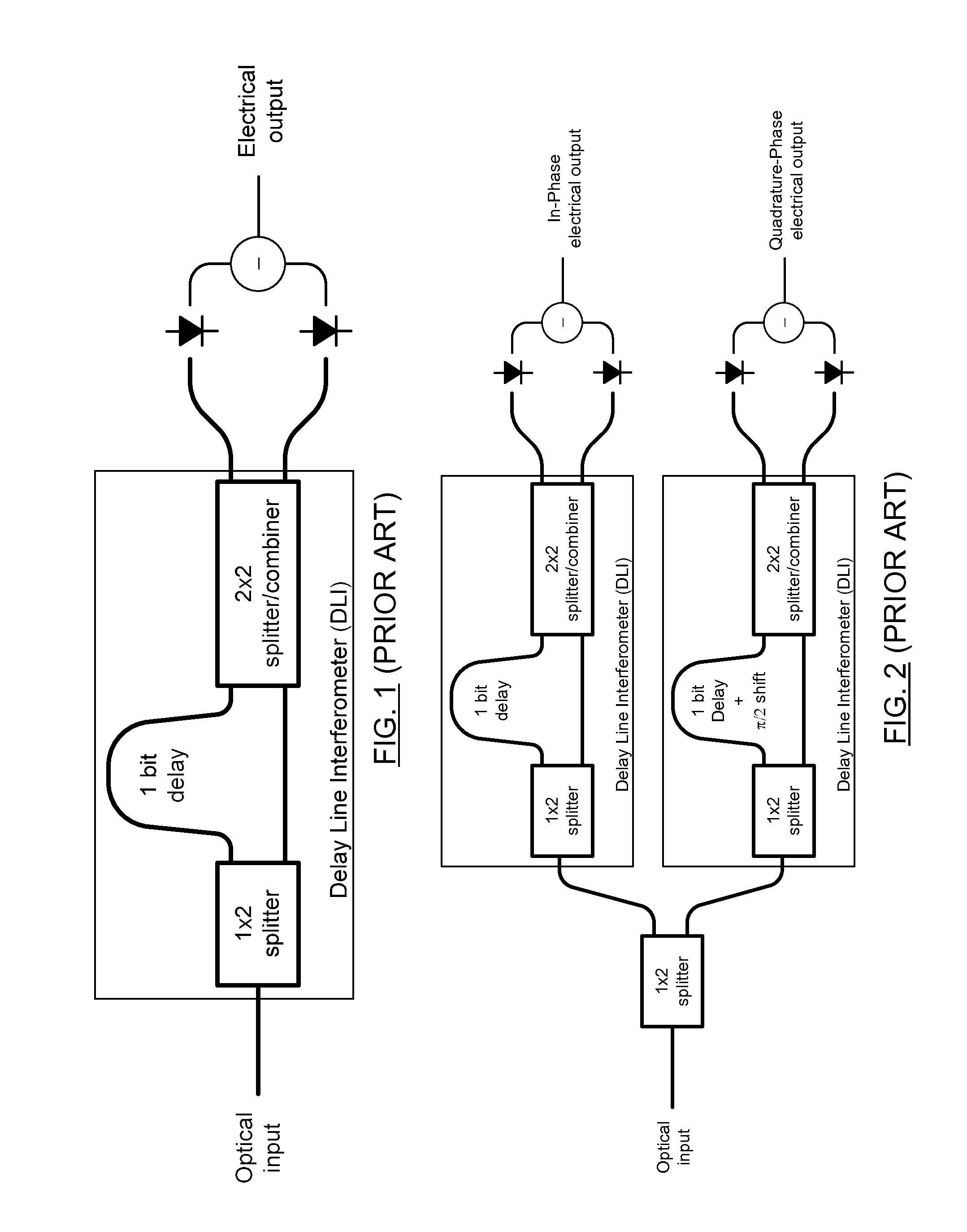
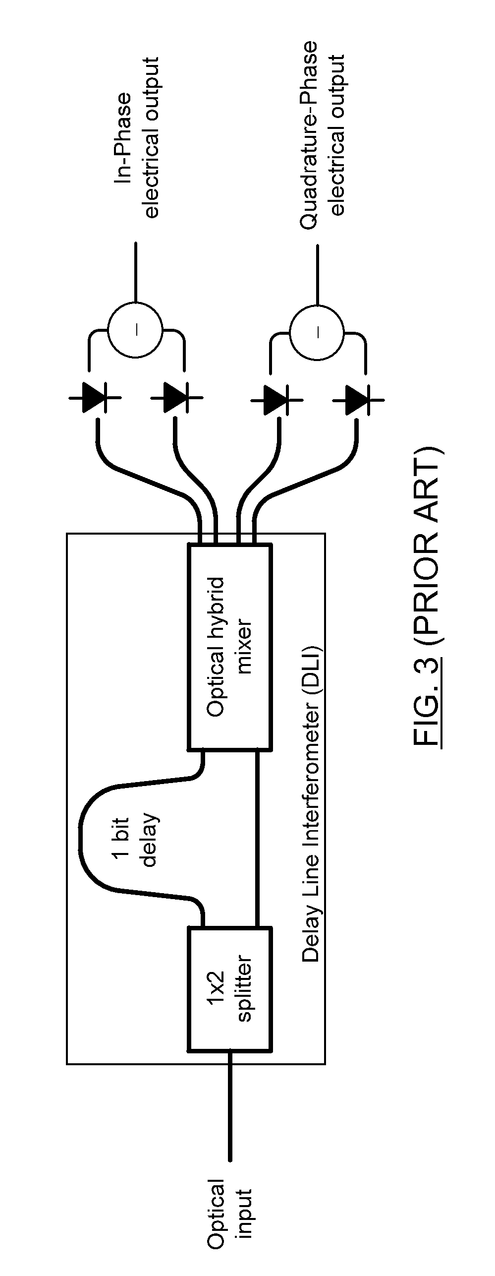
[0042]In the following description, similar features in the drawings have been given similar reference numerals, and, in order to not unduly encumber the figures, some elements may not be indicated on some figures if they were already identified in preceding figures. It should also be understood herein that the elements of the drawings are not necessarily depicted to scale, since emphasis is placed upon clearly illustrating the elements and structures of the present embodiments.

Polarization-Insensitive Optical Receiver

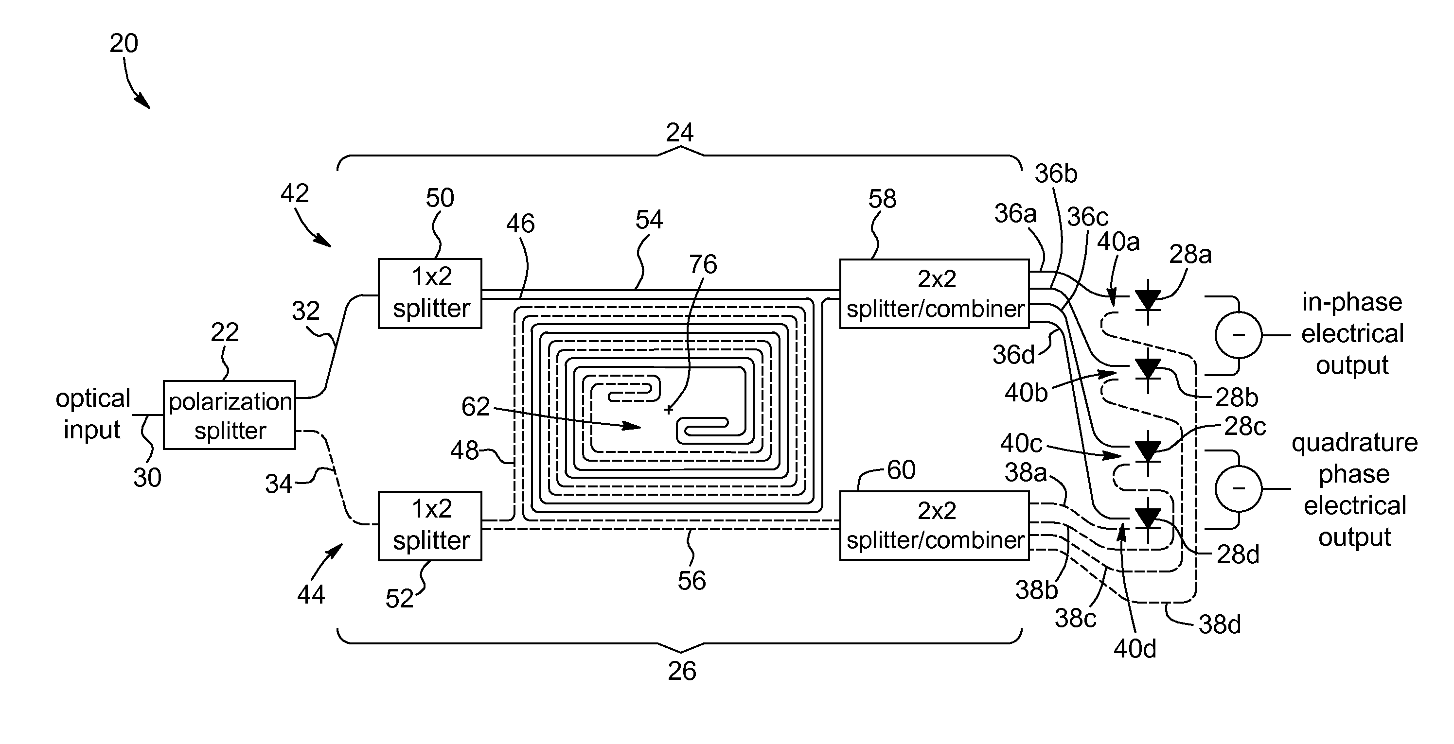
[0043]In accordance with an aspect of the invention, there is provided a polarization-insensitive optical receiver for demodulating a phase-modulated input optical signal.

[0044]Throughout the present description, the expression “polarization-insensitive”, when used to characterize the optical receiver according to embodiments of the invention, is understood to refer to an optical receiver capable of demodulating the phase-modulated input optical signal independently of...


PUM


Abstract

A polarization-insensitive optical receiver for demodulating a phase-modulated input optical signal is provided. The optical receiver includes successively a polarization splitter, a first and second interferometric modules including respective delay lines, and a plurality of detectors. The input optical signal is split into two substantially orthogonally-polarized components, which are launched along respective optical paths into the corresponding interferometric modules where they demodulated and subsequently recombined prior to being detected by the plurality of detectors. Advantageously, the optical receiver allows mitigating undesired discrepancies between the optical paths traveled by the two polarization components by arranging the respective delay lines of the interferometric modules into intertwined spiraling structures. A waveguide assembly including a substrate and a pair of waveguides on the substrate and defining intertwined spiraling structures is also provided, as well as a waveguide coupling assembly for coupling, onto a same detector, two optical signals travelling along two parallel coplanar waveguides.

Description

RELATED PATENT APPLICATION[0001]This application incorporates by reference and claims priority to U.S. provisional patent application Ser. No. 61 / 588,411, filed Jan. 19, 2012.FIELD OF THE INVENTION[0002]The present invention relates to the field of optical components and more particularly concerns improvements useful for optical receivers for telecommunication systems, and the like.BACKGROUND[0003]As telecommunication systems have evolved from 10-gigabit-per-second (Gb / s) data transfer rates to 40 Gb / s and now toward 100 Gb / s, it has been desirable to develop more sophisticated modulation schemes. As a result, over the past decades, modulation of optical signals has gradually changed from simple amplitude on-off keying to more advanced modulation formats, such as phase modulation. At transmission rates of 40 Gb / s and higher, phase modulation schemes such as differential phase-shift keying (DPSK) and differential quadrature phase-shift keying (DQPSK) are now typically used. Such adva...

Claims


Application Information

Patent Timeline
Patent Type & Authority Applications(United States)
IPC IPC(8): H04B10/06G02B6/34G02B6/12G02B6/26
CPCH04B10/612G02B6/12G02B6/26G02B6/126H04B10/677G02B6/12004G02B6/34
Inventor PAINCHAUD, YVES
Owner CIENA
Why Eureka
Try Eureka