
Device for improving performance in sted and resolft microscopy using a single phase mask
a technology of resolft microscopy and sted, which is applied in the field of phase plate or spatial light modulator, can solve the problems of reducing the efficiency of secondary excitation areas, significantly weaker improvement of lateral resolution, and limiting the resolution of fluorescence microscopy, so as to reduce the degree of freedom for alignment, improve beam quality, and minimize the effect of central intensity
- Summary
- Abstract
- Description
- Claims
- Application Information
AI Technical Summary
Benefits of technology
Problems solved by technology
Method used
Image

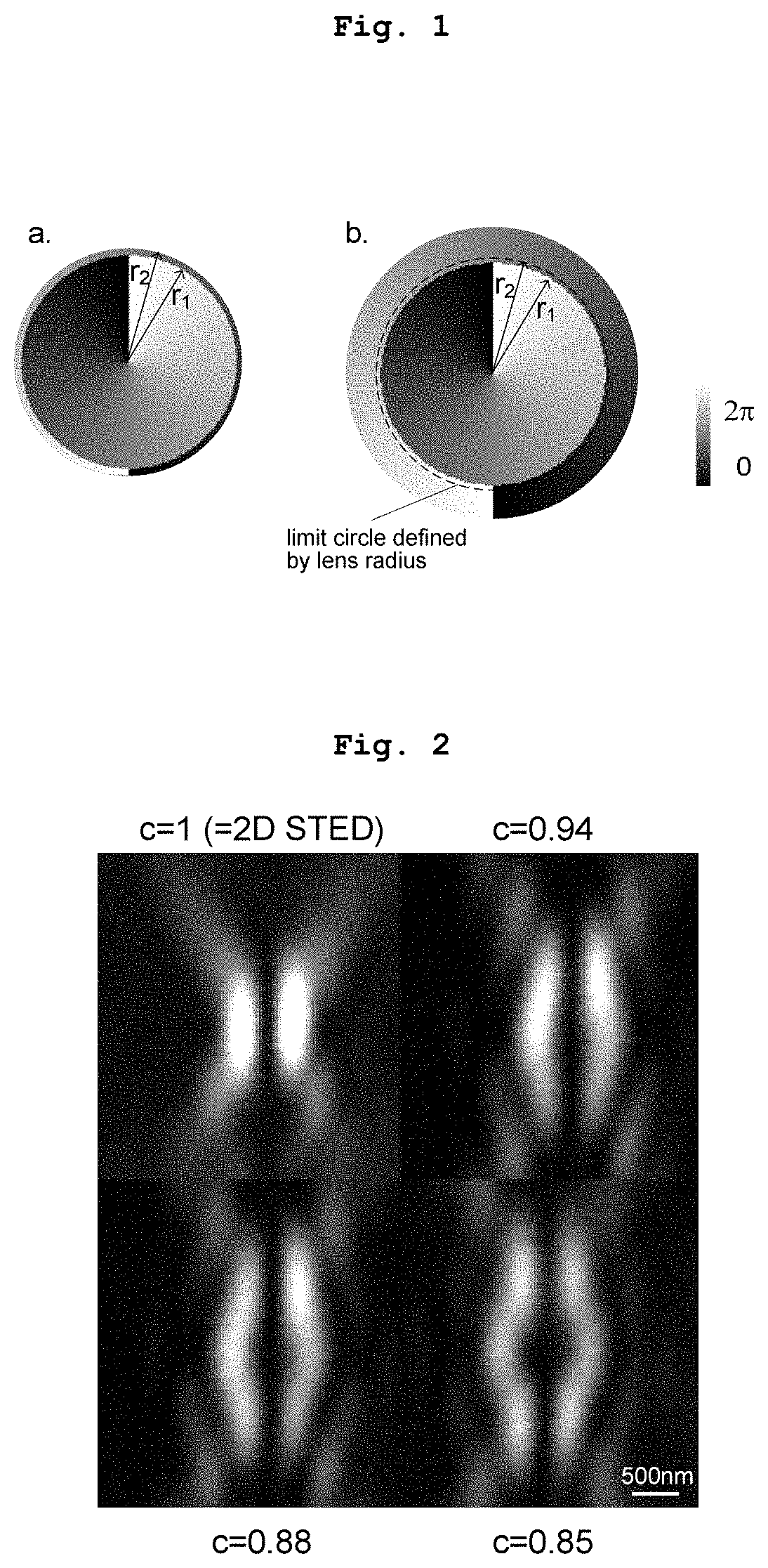
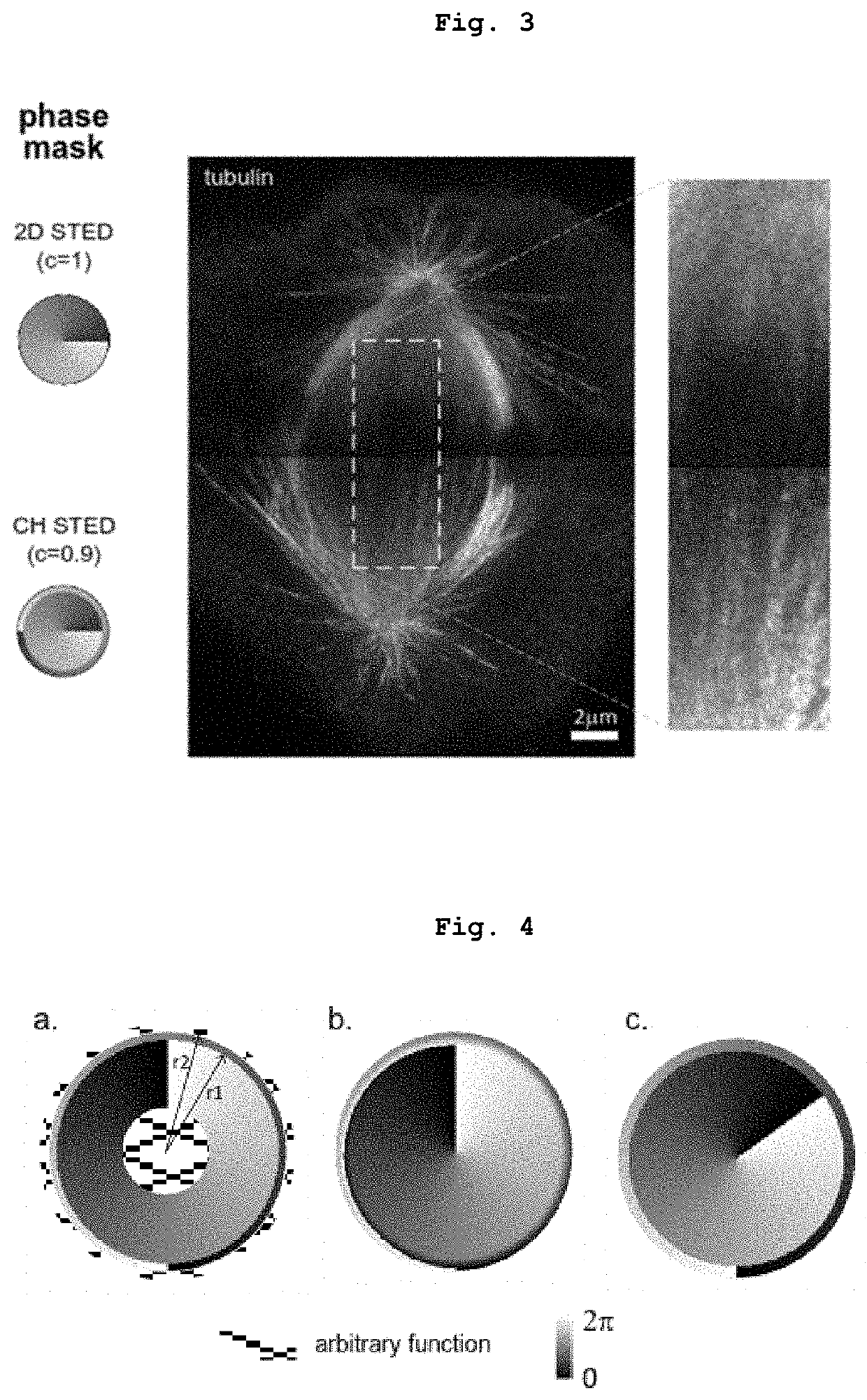
Examples
example 1
n of a Phase Plate Generating the Bivortex Phase Mask
[0044]In an example, the bivortex phase mask of the present invention is generated by a phase plate device. Such device can be produced by crafting the negative of the bivortex phase mask of the present invention's phase plate onto a mold and by developing the mold to obtain a bivortex phase plate. The manufacture by molding may be achieved by methods known in the art, for example those described by Oemrawsingh et al, 2004, with the addition of comprising a step of: designing the mold as a negative of the present invention's phase mask. After release of the mold, a solid phase plate with a bivortex configuration is obtained.
example 2
n of the Bivortex Phase Mask by a Spatial Light Modulator
[0045]In another example, the bivortex phase mask of the present invention can be generated by a spatial light modulator device (SLM). Such SLM can be produced by integrating complementary metal-oxide-semiconductor (CMOS) in the SLM, by methods such as the ones described in the art (ZHU, et al 2004.), with the addition of comprising a step of: imprinting the present invention's bivortex phase mask onto the SLM, through electronic control of its subunits.
example 3
oscopy Method Employing a Bivortex Phase Mask Through Compensation or Correction Functions
[0046]Another example of an embodiment of the present invention refers to a method for STED microscopy that can be developed through comprising a step of: modulating the physical phase of a radiation beam on an existing phase plate or a spatial light modulator using compensation or corrective phase functions to ultimately generate the present invention's byvortex phase mask as the effective phase mask.
PUM
| Property | Measurement | Unit |
|---|---|---|
| distance | aaaaa | aaaaa |
| angle | aaaaa | aaaaa |
| phase | aaaaa | aaaaa |
Abstract
Description
Claims
Application Information