Method of manufacturing display apparatus, display apparatus, and structure for manufacturing display apparatus

Active Publication Date: 2021-07-15
SAMSUNG ELECTRONICS CO LTD
View PDF0 Cites 1 Cited by
  • Summary
  • Abstract
  • Description
  • Claims
  • Application Information

AI Technical Summary

Benefits of technology

[0005]According to an embodiment of the disclosure, provided is a method of manu

Problems solved by technology

However, a chip bonded to the driving substrate is firmly bonded to the driving substrate by soldering, and thus, the chip may not be easily removed from the driving substrate.
Because the micro-LED chi

Method used


Image

  • Method of manufacturing display apparatus, display apparatus, and structure for manufacturing display apparatus
  • Method of manufacturing display apparatus, display apparatus, and structure for manufacturing display apparatus
  • Method of manufacturing display apparatus, display apparatus, and structure for manufacturing display apparatus

Examples


Example

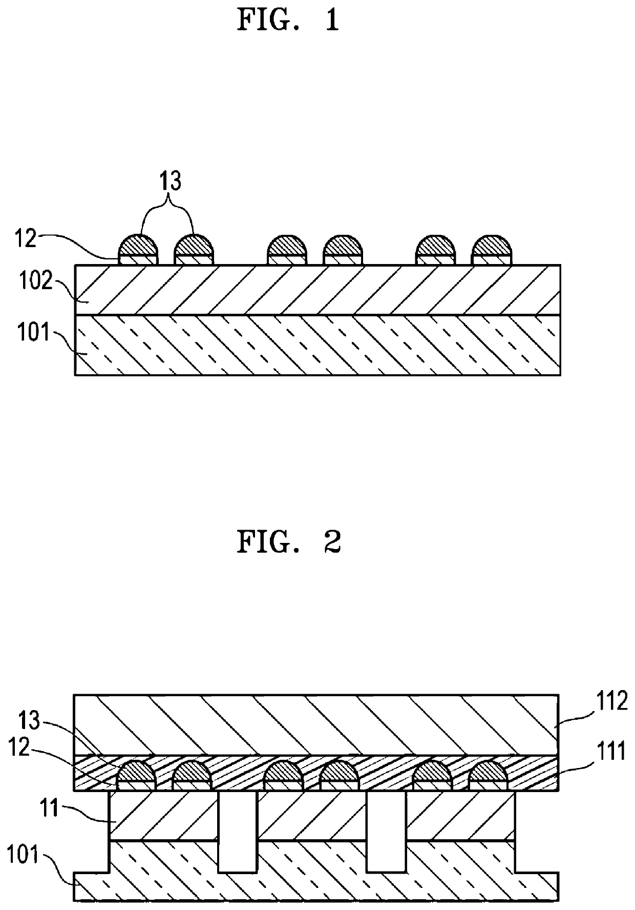
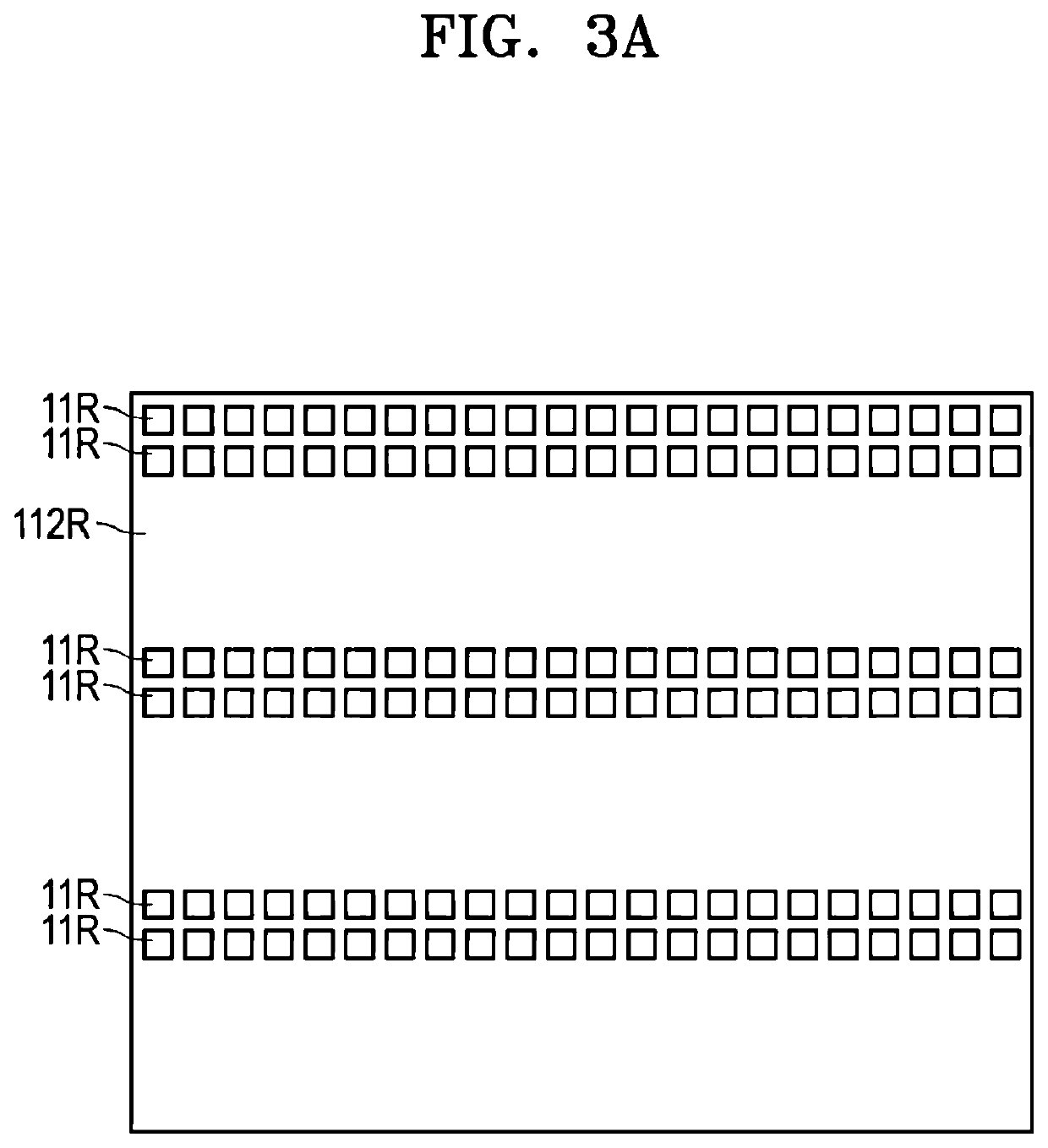
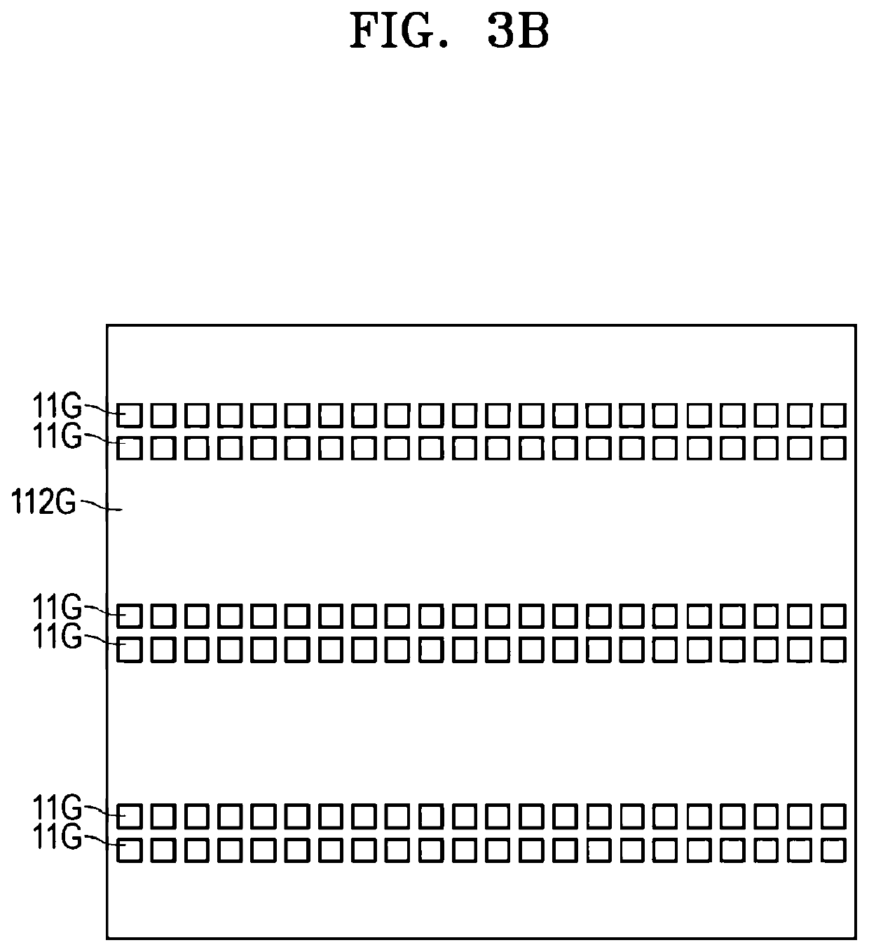
[0046]Hereinafter, the disclosure will be described with reference to the accompanying drawings, in which one or more embodiments of the disclosure are shown. The same reference numerals in the drawings denote the same elements, and sizes of elements in the drawings may be exaggerated for clarity and convenience of explanation. In addition, embodiments of the disclosure described hereinbelow are merely examples, and various modifications may be made from the embodiments of the disclosure.

[0047]Throughout the disclosure, the expression “at least one of a, b or c” indicates only a, only b, only c, both a and b, both a and c, both b and c, all of a, b, and c, or variations thereof.

[0048]It will be understood that when an element is referred to as being “above” or “on” another element, it may be directly on the other element, or intervening elements may be present therebetween. Likewise, it will also be understood that when an element is referred as being “under” or “below” another elem...


PUM


Abstract

A method of manufacturing a display apparatus, a display apparatus, and a structure for manufacturing a display apparatus are provided. The method of manufacturing a display apparatus includes: forming a micro-light-emitting diode (LED) chip on a relay substrate such that a chip-side electrode is exposed; transferring the micro-LED chip from the relay substrate to a driving substrate including a driving substrate-side electrode; and bonding the chip-side electrode to the driving substrate-side electrode.

Description

CROSS-REFERENCE TO RELATED APPLICATION(S)[0001]This application claims the benefit of Japanese Patent Application No. 2020-003723, filed on Jan. 14, 2020, in the Japanese Patent Office and Korean Patent Application No. 10-2020-0023837, filed on Feb. 26, 2020, in the Korean Intellectual Property Office, the disclosures of which are incorporated herein by reference in their entireties.BACKGROUND1. Field[0002]The disclosure relates to a method of manufacturing a display apparatus, a display apparatus, and a structure for manufacturing a display apparatus.2. Description of Related Art[0003]Recently, display apparatuses using micro-light-emitting diodes (LEDs) as light-emitting devices have been in the spotlight. Micro-LED display apparatuses (hereinafter, referred to as “display apparatuses”) are next-generation display apparatuses that are capable of displaying high-luminance and high-quality images at low power without causing a decrease in response speed. In display apparatus manufac...

Claims


Application Information

Patent Timeline
IPC IPC(8): H01L27/15G09F9/33
CPCH01L27/156G09F9/33H01L25/0753H01L33/62H01L2933/0066
Inventor TAKAGI, TAKASHIWADA, MASARUYANAGISAWA, SATOSHIFUJIWARA, TSUBASA
Owner SAMSUNG ELECTRONICS CO LTD
Why Eureka
Try Eureka