Supercharge Your Innovation With Domain-Expert AI Agents!

Method and image processing device for mura detection on display

a technology of image processing and display screen, applied in image analysis, image enhancement, instruments, etc., can solve the problems of affecting the user's viewing of display contents, and affecting the display screen performan

Active Publication Date: 2022-02-03
NOVATEK MICROELECTRONICS CORP
View PDF9 Cites 0 Cited by
  • Summary
  • Abstract
  • Description
  • Claims
  • Application Information

AI Technical Summary

Benefits of technology

This patent proposes a method and device for detecting mura defects on a display. The method includes segmenting the original image of the display into smaller parts, filtering out a specific range of spatial frequency components from these parts to create filtered parts, and identifying the mura defect based on the filtered parts and pre-defined patterns. This approach is designed to improve the detection and inspection of mura defects during manufacturing of display panels. The device includes a memory and processing circuit for implementing this method. Overall, this technology helps to improve the manufacturing process of display panels by detecting and eliminating mura defects.

Problems solved by technology

“Mura” defects on a display screen are contrast-type defects which appear as non-uniform brightness regions due to manufacture and assembly errors, where one or more pixels are brighter or darker than surrounding pixels.
Such defects would impede the performance of the display screen and distract the user from viewing of display contents.
However, the solutions for organic light-emitting diode displays (OLED displays) have not been addressed.
Mura on OLED displays normally appear with different shapes and sizes and are extremely difficult to be measured since they are hardly to be distinguished from the background.
Moreover, most existing mura detection methods are done through human visual inspection that is subjective, inconsistent, and inefficient, and therefore different types of mura are not able to be properly classified and labelled for demura processes.

Method used


Image

  • Method and image processing device for mura detection on display
  • Method and image processing device for mura detection on display
  • Method and image processing device for mura detection on display

Examples


Embodiment Construction

[0018]Some embodiments of the disclosure will now be described more fully hereinafter with reference to the accompanying drawings, in which some, but not all embodiments of the application are shown. Indeed, various embodiments of the disclosure may be embodied in many different forms and should not be construed as limited to the embodiments set forth herein; rather, these embodiments are provided so that this disclosure will satisfy applicable legal requirements. Like reference numerals refer to like elements throughout.

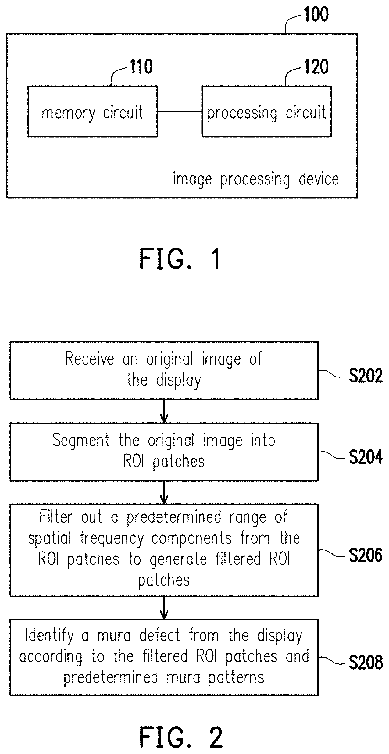
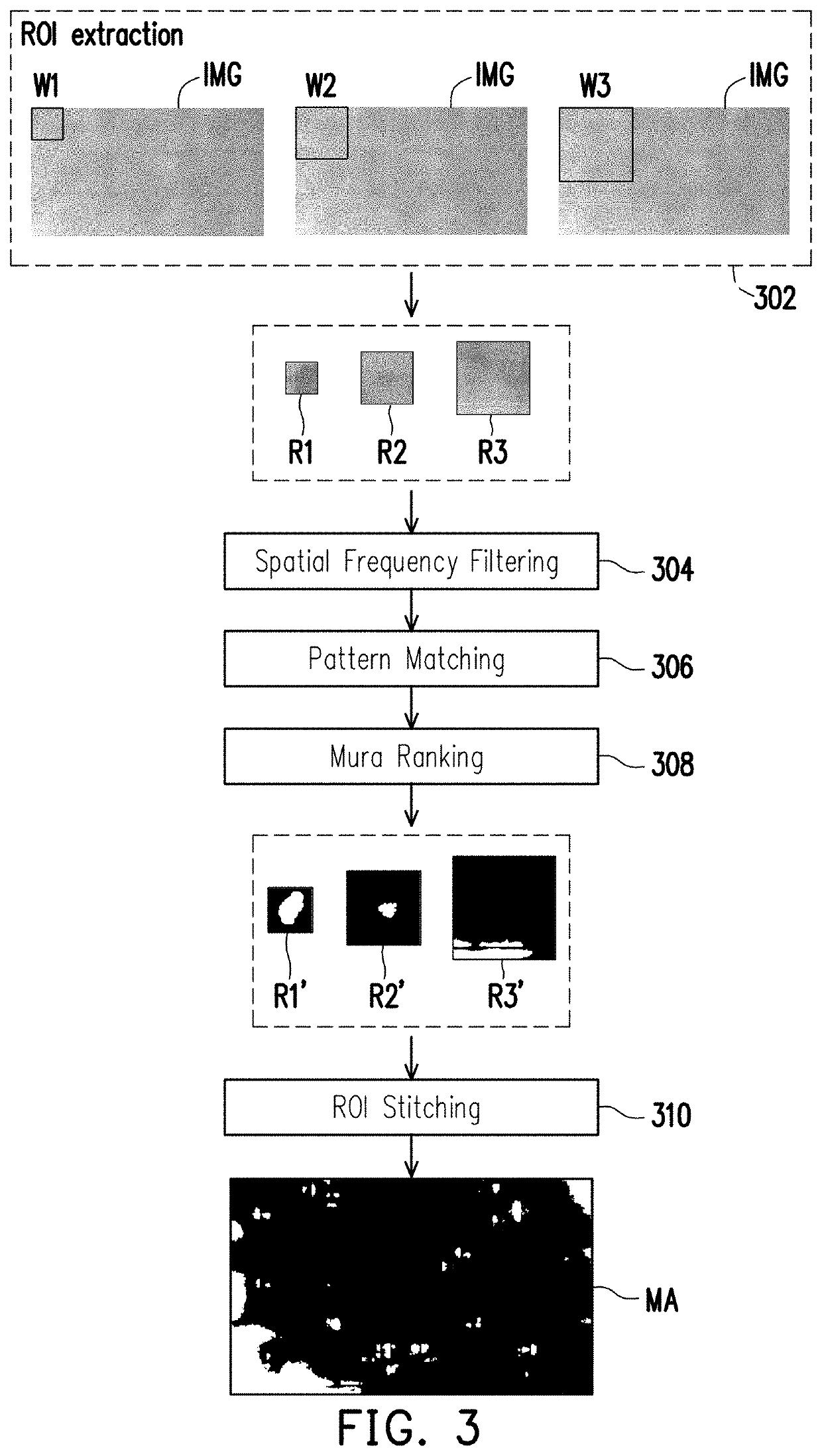
[0019]FIG. 1 illustrates a schematic diagram of a proposed image processing device in accordance with one of the exemplary embodiments of the disclosure. All components of the image processing device and their configurations are first introduced in FIG. 1. The functionalities of the components are disclosed in more detail in conjunction with FIG. 2.

[0020]Referring to FIG. 1, an image processing device 100 for mura detection on a display would include a memory circui...


PUM


Abstract

A method and an image processing device for mura detection on a display are proposed. The method includes the following steps. An original image of the display is received and segmented into region of interest (ROI) patches. A predetermined range of spatial frequency components are filtered out from the ROI patches to generate filtered ROI patches. A mura defect is identified from the display according to the filtered ROI patches and predetermined mura patterns.

Description

TECHNICAL FIELD[0001]The disclosure relates to a technique for mura detection on a display.BACKGROUND[0002]“Mura” defects on a display screen are contrast-type defects which appear as non-uniform brightness regions due to manufacture and assembly errors, where one or more pixels are brighter or darker than surrounding pixels. Such defects would impede the performance of the display screen and distract the user from viewing of display contents.[0003]Mura detection on thin-film transistor liquid-crystal diode displays (TFT-LCDs) has been maturely developed. However, the solutions for organic light-emitting diode displays (OLED displays) have not been addressed. Mura on OLED displays normally appear with different shapes and sizes and are extremely difficult to be measured since they are hardly to be distinguished from the background. Moreover, most existing mura detection methods are done through human visual inspection that is subjective, inconsistent, and inefficient, and therefore ...

Claims


Application Information

Patent Timeline
IPC IPC(8): G06T7/00G06T7/11G06K9/62G06T5/20
CPCG06T7/001G06T7/11G06T2207/30168G06T5/20G06K9/6215G06V10/25G06T7/0002G06T2207/20021G06V10/761G06F18/22
Inventor CHU, CHIH-YUHSIEH, PO-YUANLEE, CHIEH-ENTIEN, CHUNG-HAOCHEN, SHIH-HSUAN
Owner NOVATEK MICROELECTRONICS CORP
Features
  • R&D
  • Intellectual Property
  • Life Sciences
  • Materials
  • Tech Scout
  • Unparalleled Data Quality
  • Higher Quality Content
  • 60% Fewer Hallucinations
Learn More