Signal integration circuit and electronic device

Pending Publication Date: 2022-11-10
GETAC TECH CORP
View PDF3 Cites 0 Cited by
  • Summary
  • Abstract
  • Description
  • Claims
  • Application Information

AI Technical Summary

Benefits of technology

The present invention provides a signal integration circuit and electronic device that can receive multiple input signals simultaneously and filter out signals that overlap with a specific band. These signals are then integrated into one output signal that can be sent to one input port of a communication module. This reduces the number of input ports needed for the communication module without affecting the speed at which input signals are downloaded or the sensitivity of the device to the specific band.

Problems solved by technology

However, this severely affects communication quality of the electronic products.

Method used


Image

  • Signal integration circuit and electronic device
  • Signal integration circuit and electronic device

Examples


Embodiment Construction

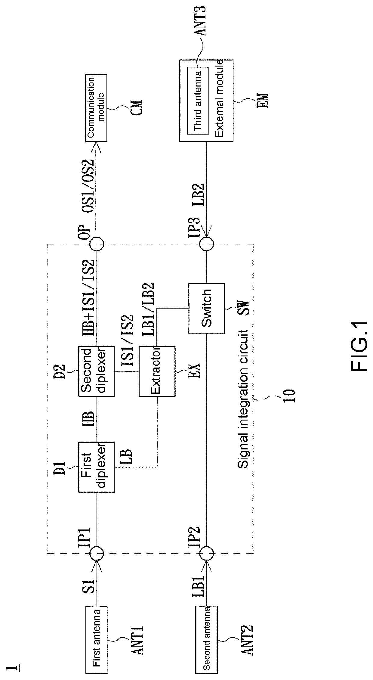
[0012]Referring to FIG. 1, FIG. 1 shows a block schematic diagram of an electronic device according to an embodiment of the present invention. An electronic device 1 includes a communication module CM, an external module EM and a signal integration circuit 10. The signal integration circuit 10 includes a first input port IP1, a second input port IP2, a third input port IP3 and an output port OP. The first input port IP1 is for inputting (receiving) an input signal S1, wherein the input signal S1 includes a high band (e.g., 3.3 GHz to 5.9 GHz) signal HB and a low band (e.g., 617 MHz to 2.69 GHz) signal LB. The second input port IP2 is for inputting a first L1 band (e.g., 1.56 GHz to 1.61 GHz) signal LB1, and the third input port IP3 is for inputting a second L1 band (e.g., 1.56 GHz to 1.61 GHz) signal LB2, wherein the band of the second L1 band signal LB2 preferably overlaps with the band of the first L1 band signal LB1. Moreover, the first L1 band signal LB1 has an overlapping band ...


PUM


Abstract

An electronic device includes a communication module, an external module and a signal integration circuit. The signal integration circuit includes a first input port, a second input port, a third input port and an output port. The first input port is for inputting an input signal. The second input port is for selectively inputting a first L1 band signal. The third input port is for selectively inputting a second L1 band signal. The output port selectively outputs a first output signal or a second output signal. When the third input port is coupled to an external module, the third input port is for inputting the second L1 band signal, and the output port outputs the second output signal. When the third input port is not coupled to the external module, the second input port is for inputting the first L1 band signal, and the output port outputs the first output signal.

Description

[0001]The application claims priority to U.S. Provisional Application No. 63 / 184,100, filed on May 4, 2021, the disclosure of which is hereby incorporated by reference herein in its entirety.BACKGROUND OF THE INVENTIONField of the Invention[0002]The present invention relates to signal integration and, more particularly, to a signal integration circuit and an electronic device capable of integrating multiple received input signals into one output signal.Description of the Prior Art[0003]With the thriving development of wireless broadband networks and mobile communication technologies, electronic products equipped with numerous different communication functions and external antenna modules are extensively applied, such that the number of antenna elements is also ever-increasing along with the evolving communication technologies. However, this severely affects communication quality of the electronic products.SUMMARY OF THE INVENTION[0004]In view of the above, a signal integration circu...

Claims


Application Information

Patent Timeline
IPC IPC(8): H04B1/12H04B1/40H03F3/189
CPCH04B1/12H04B1/40H03F3/189H03F2200/294H03F2200/451Y02D30/70H04B7/0808H04B7/082H04B7/0613H04L9/40
Inventor WANG, MIN-YUCHEN, KUAN-YU
Owner GETAC TECH CORP
Why Eureka
Try Eureka