Signal integration circuit and electronic device

Pending Publication Date: 2022-11-10
GETAC TECH CORP
View PDF2 Cites 0 Cited by
  • Summary
  • Abstract
  • Description
  • Claims
  • Application Information

AI Technical Summary

Benefits of technology

The present invention provides a signal integration circuit and an electronic device that can simultaneously receive multiple different input signals, filter out signals of the same band, and integrate them into one output signal. This reduces the number of input ports of a communication module and improves the reception of L1 and L5 bands.

Problems solved by technology

With the development of wireless broadband networks and mobile communication technologies, electronic products equipped with numerous different communication functions and external antenna modules are extensively applied, such that the number of antenna elements is also ever-increasing along with the evolving communication technologies, and this however severely affects the communication quality of electronic products.
In addition, different antenna types can change circuit diagrams, layouts and routings, hence increasing costs and design time.

Method used


Image

  • Signal integration circuit and electronic device
  • Signal integration circuit and electronic device
  • Signal integration circuit and electronic device

Examples


first embodiment

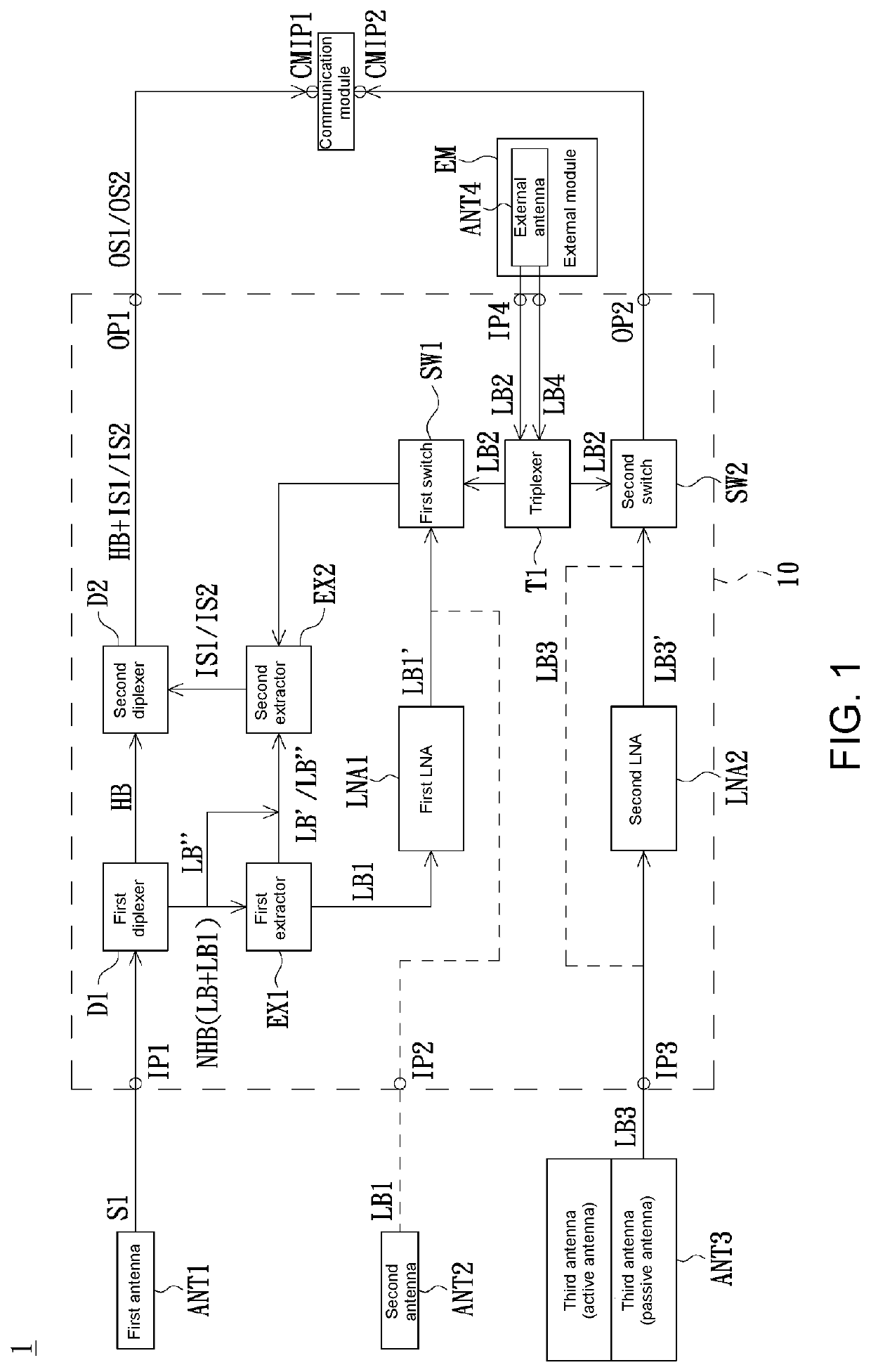
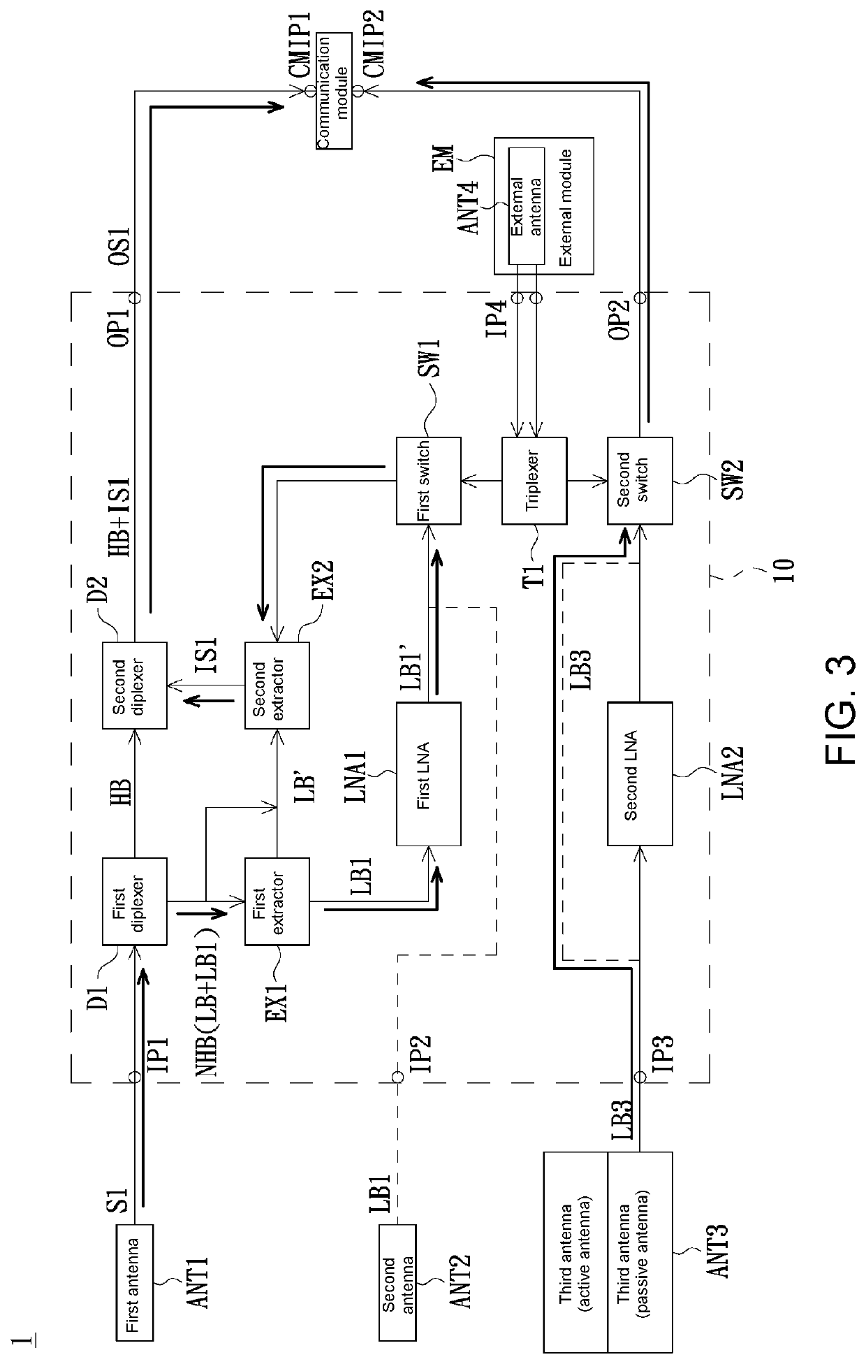
[0027]Refer to FIG. 2 to FIG. 5 showing schematic diagrams of signal paths according to four embodiments of the present invention. In the first embodiment, as shown in FIG. 2, the first L1 band signal LB1 is inputted via the second antenna ANT2, and can be directly transmitted into the first switch SW1 without an LNA since the second antenna ANT2 is an active antenna. After the first L1 band signal LB1 passes through the first switch SW1, the first L1 band signal LB1 is integrated with the low band signal LB″ excluding the overlapping band signal by the second extractor EX2 into the first integrated signal IS1; the high band signal HB and the first integrated signal IS1 are then combined by the second diplexer D2 into the first output signal OS1 that is then transmitted to the first output port OP1 and the first input port CMIP1 of the communication module. The first L5 band signal LB3 is inputted via the passive antenna of the third antenna group ANT3, and is amplified by the secon...

second embodiment

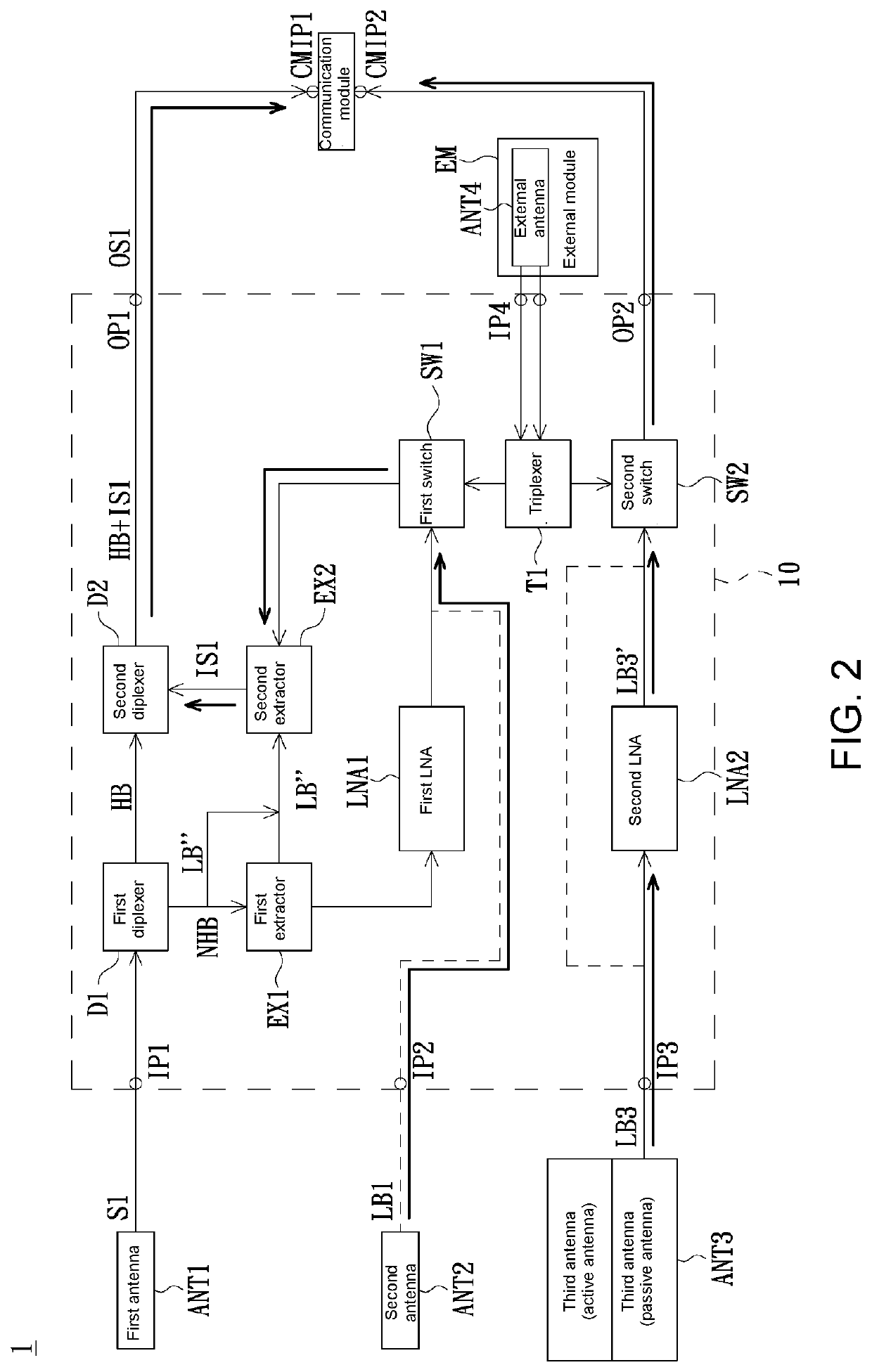
[0028]In the second embodiment, as shown in FIG. 3, the input signal S1 is inputted via the first antenna ANT1, and is separated into the high band signal HB and the non-high band signal NHB by the first diplexer D1, wherein the non-high band signal NHB is separated into the low band signal LB and the first L1 band signal LB1 by the first extractor EX1. At the same time, the first extractor EX1 filters out the signal existing in the overlapping band (i.e., 1.563 GHz to 1.61 GHz) from the low band signal LB so that the energy of such signal is minimized or even approaches zero, outputs the first L1 band signal LB1 from the first output terminal, and outputs the low band signal LB′ from which the overlapping band signal is filtered out from the second output terminal. The first L1 band signal LB1 is amplified by the first LNA LNA1 into the amplified first L1 band signal LB1′ and transmitted to the first switch SW1, and is selectively outputted to the second extractor EX2 by the first ...

third embodiment

[0029]In the third embodiment, as shown in FIG. 4, the first L1 band signal LB1 is inputted via the second antenna ANT2, and can be directly transmitted into the first switch SW1 without needing an LNA since the second antenna ANT2 is an active antenna. The first switch SW1 selectively outputs the first L1 band signal LB1 to the second extractor EX2. The second extractor EX2 integrates the first L1 band signal LB1 and the low band signal LB″ excluding the overlapping band signal into the first integrated signal IS1, and transmits the first integrated signal IS1 to the second diplexer D2. The second diplexer D2 combines the high band signal HB and the first integrated signal IS1 into the first output signal OS1 and transmits the first integrated output signal OS1 to the first output port OP1 and the first input port CMIP1 of the communication module. The first L5 band signal LB3 is inputted via the active antenna of the third antenna group ANT3, and can be directly transmitted to the...


PUM


Abstract

An electronic device provided includes a communication module, an external module, and a signal integration circuit including first to fourth input ports, and first and second output ports. The first input port is for inputting an input signal. The second input port is for inputting a first L1 band signal. The third input port is for inputting a first L5 band signal. The fourth input port is for inputting a second L1 band signal and a second L5 band signal. The first output port selectively outputs a first output signal and a second output signal. The second output port selectively outputs the first L5 band signal and the second L5 band signal. When the fourth input port is not coupled to an external module, the first output port outputs the first output signal, and the second output port outputs the first L5 band signal.

Description

[0001]The application claims priority to U.S. Provisional Application No. 63 / 184,100, filed on May 4, 2021, the disclosure of which is hereby incorporated by reference herein in its entirety.BACKGROUND OF THE INVENTIONField of the Invention[0002]The present invention relates to a signal integration circuit and an electronic device, and more particularly, to a signal integration circuit and an electronic device capable of integrating multiple received input signals into to two output signals.Description of the Prior Art[0003]With the development of wireless broadband networks and mobile communication technologies, electronic products equipped with numerous different communication functions and external antenna modules are extensively applied, such that the number of antenna elements is also ever-increasing along with the evolving communication technologies, and this however severely affects the communication quality of electronic products. In addition, different antenna types can cha...

Claims


Application Information

Patent Timeline
IPC IPC(8): H04L9/40H04B7/06
CPCH04L29/06H04B7/0613H04B1/40H04B1/12Y02D30/70H04B7/0808H04B7/082H04L9/40H03F3/189H03F2200/294H03F2200/451
Inventor WANG, MIN-YU
Owner GETAC TECH CORP
Why Eureka
Try Eureka