Detection method and apparatus for reduced cross -talk and asic area of a fingerprint sensor

a fingerprint sensor and detection method technology, applied in the field of detection methods and apparatus for reducing crosstalk and asic area of fingerprint sensors, can solve the problems of increasing the cost of assembling the two parts, the cost of every interface signal, and the overall cost of the components of such so as to reduce the cost of a finger print sensor. , the effect of reducing the number of input and outputs/electronic connections

Active Publication Date: 2015-04-30
IDEX BIOMETRICS ASA
View PDF1 Cites 10 Cited by
  • Summary
  • Abstract
  • Description
  • Claims
  • Application Information

AI Technical Summary

Benefits of technology

[0013]Another object of the present invention is to provide a method and an apparatus for reduced number of input and outputs / electronic connections between the Sensor Substrate and an electronic circuit as a way to obtain a reduced cost of a finger print sensor (or sensor for detection of other physical or chemical characteristics of the finger without reducing the biometric performance of the finger print sensor.
[0014]Another object of the present invention is to provide a method and an apparatus for a two-dimensional fingerprint sensor with a strongly reduced number of interface connections between the Sensor Substrate containing a number of Sensor Elements and the electronic circuit in relation to the total number of Sensor Electrodes Sensor Elements (or pixels) of the Sensor Area (1).

Problems solved by technology

However, although the overall cost of the components of such a finger print sensor, consisting of a Sensor Substrate and an Electronic Circuit can be significantly lower than a corresponding solution based on a single-chip solution, the cost of assembling the two parts will increase the cost of the finished finger print sensor, in spite of the continuously reduced cost levels of such assembly processes in volume manufacture of today.
One important cost factor is related to the electric connections between such a Sensor Substrate and the Electronic Circuit.
Additionally, on the electronic circuit there is also a cost associated with every interface signal, since every signal requires a minimum connection area, which normally cannot be utilized for other functions.

Method used


Image

  • Detection method and apparatus for reduced cross -talk and asic area of a fingerprint sensor
  • Detection method and apparatus for reduced cross -talk and asic area of a fingerprint sensor
  • Detection method and apparatus for reduced cross -talk and asic area of a fingerprint sensor

Examples


Embodiment Construction

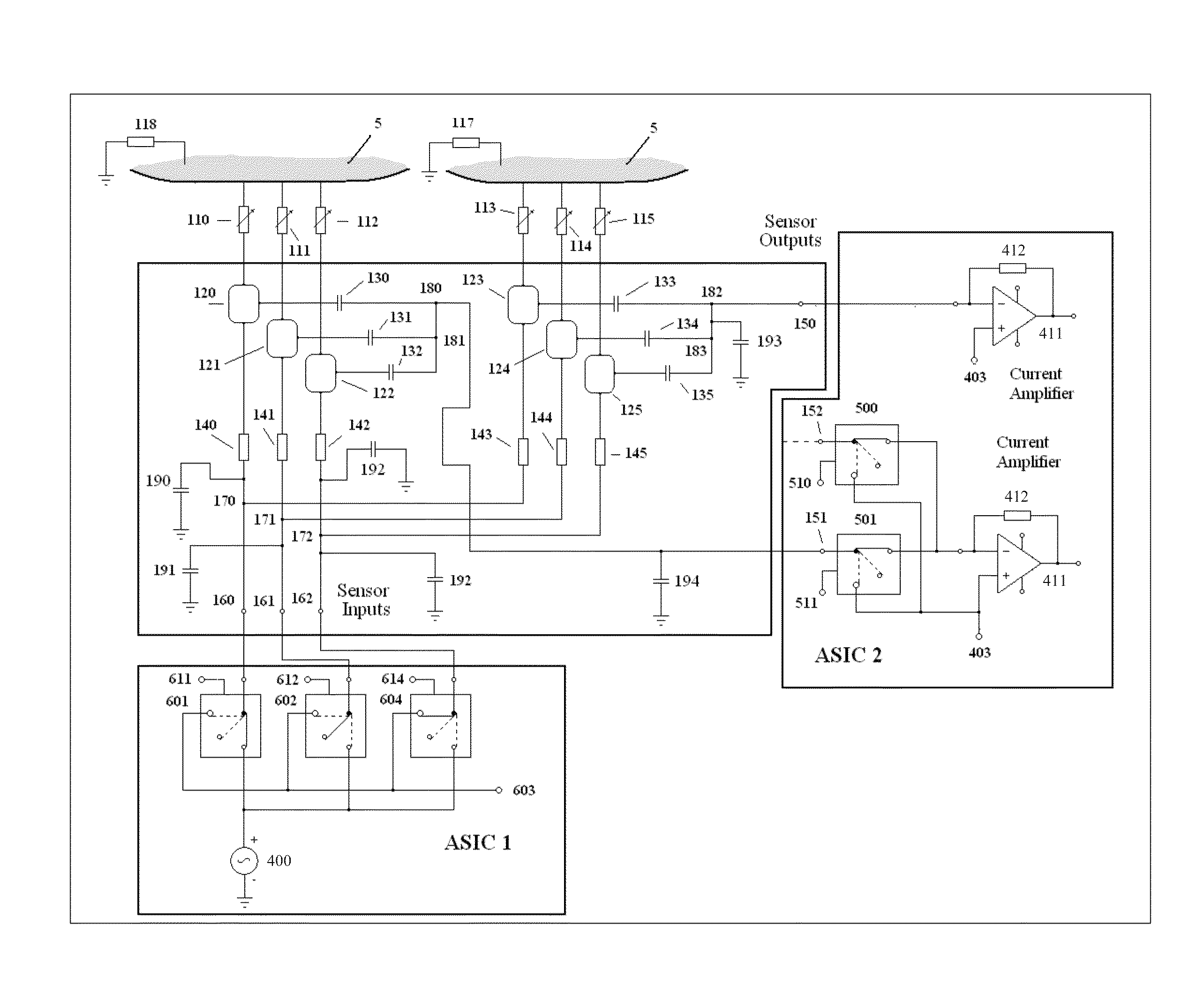
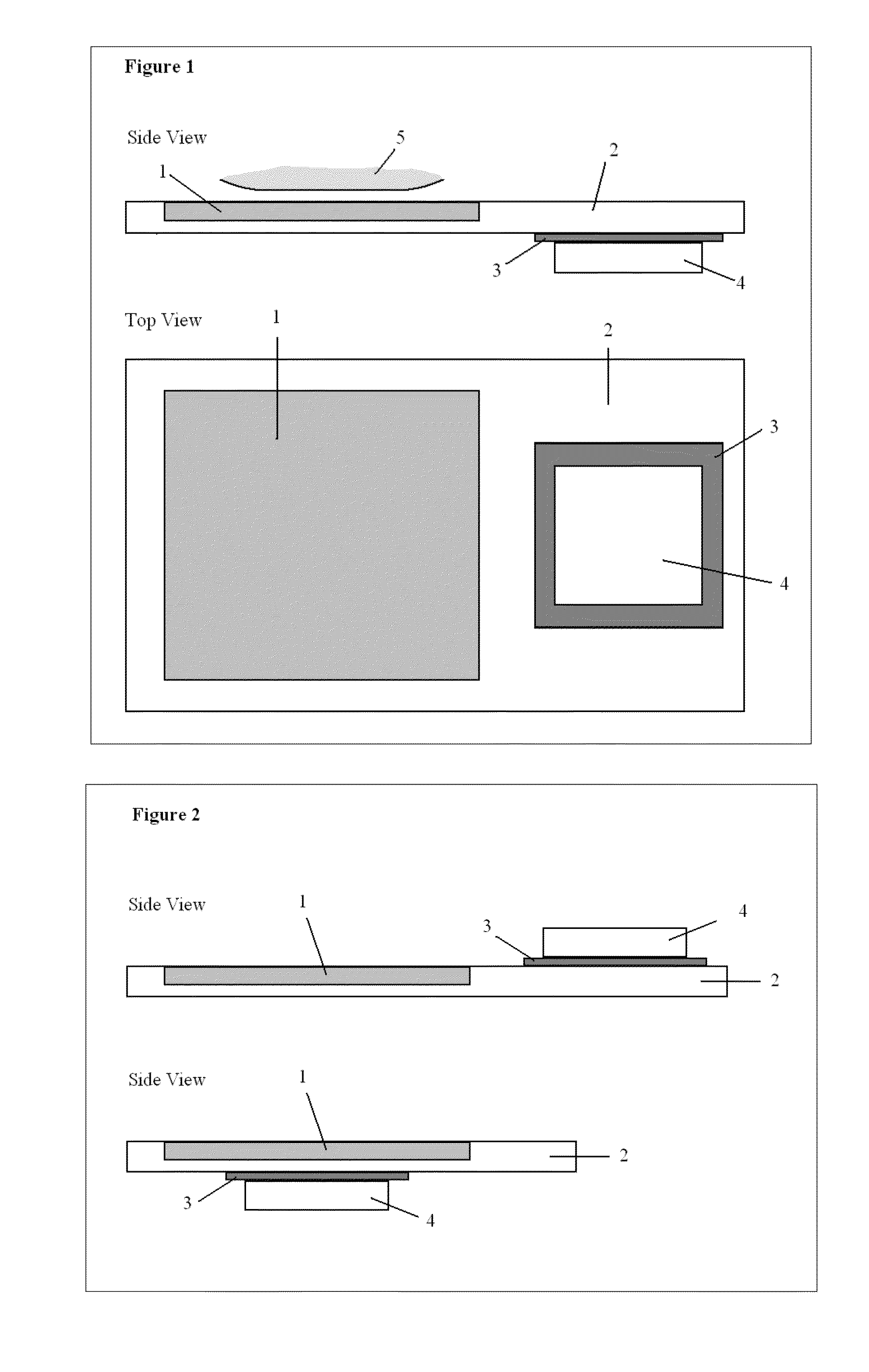
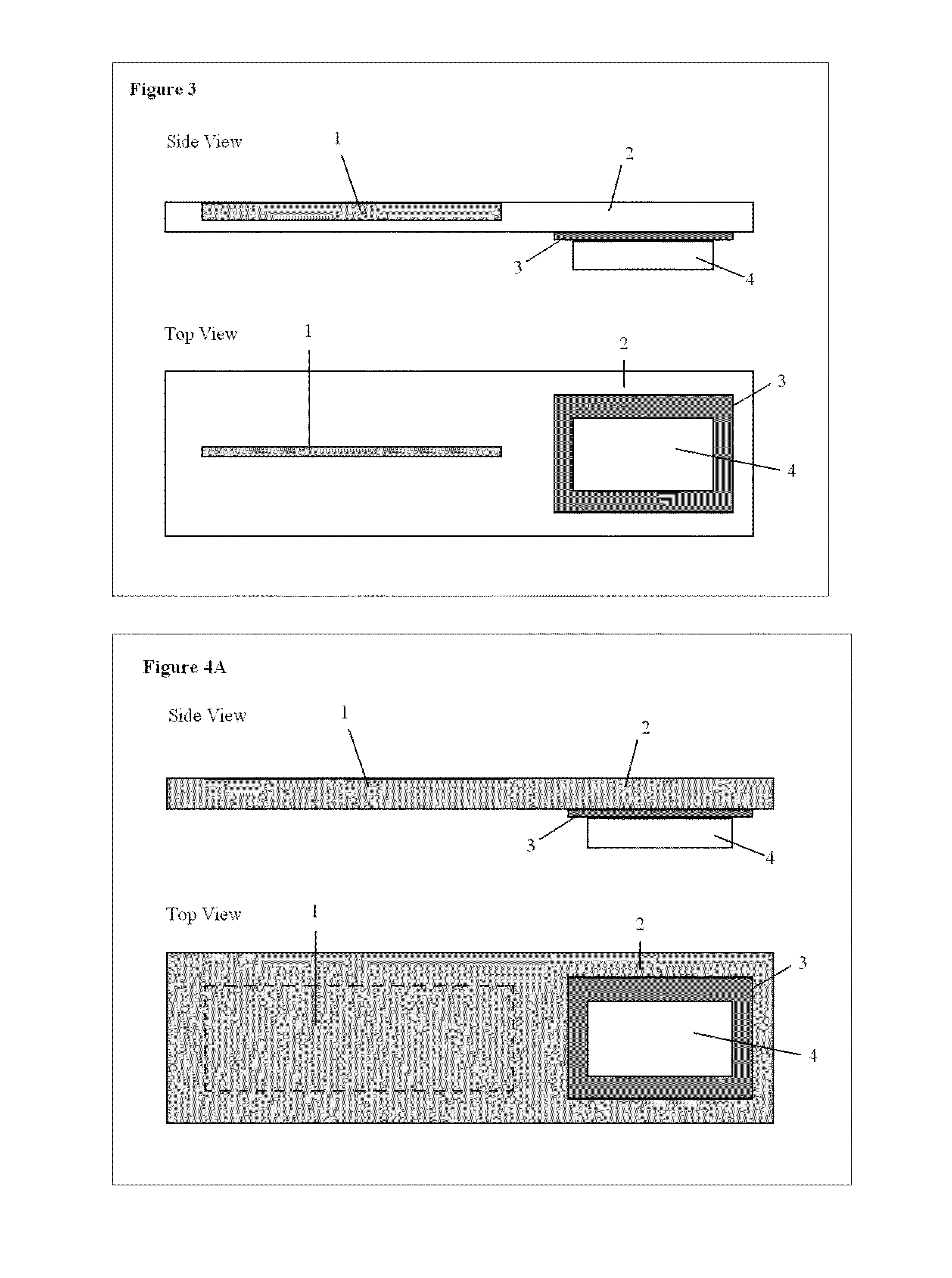
[0031]FIG. 1 shows one exemplary embodiment of the invention consisting of a Sensor Area (1) arranged for having contact with a (partially shown) Finger (5) and with means (not shown) like sensor electrodes, for sensing physical characteristics of the finger, like the surface structure and the finger print of the finger. Furthermore, the embodiment comprises an Electronic Circuit (4) being electrically connected to the Sensor Area (1) and also the sensing means, for detection of physical characteristics the finger, surface structure as well as the finger print of the finger. Both the Sensor Area (1) as well as the Electronic Circuit (4) are supported by a Carrier (2) which also provides electrical connection between the Electronic Circuit (4) and the Senor Area (1). The Carrier (2) can also physically be an integral part of the Sensor Area (1). The Electronic Circuit (4) is electrically connected to the Carrier (2) and the Sensor Area (1) and the sensing means (not shown) by a Conne...


PUM

PropertyMeasurementUnit
impedanceaaaaaaaaaa
voltageaaaaaaaaaa
currentaaaaaaaaaa

Abstract

A method and apparatus for electrical detection of a finger print has a reduced number of interconnect signals between a sensor area and a substrate and an electronic circuit for excitation and detection of the finger print compared to a single—chip finger print sensor. The individual signals are connected internally at the sensor substrate in such a way that the response from the individual sensor elements can be separated from each other. Cross-talk is reduced by keeping the sensor outputs at a constant potential, thus eliminating the effect of capacitive coupling between different sensor outputs and also between sensor outputs and a ground or reference potential.

Description

CROSS REFERENCE OF RELATED APPLICATION[0001]This application claims the benefit under 35 U.S.C. §119 of the filing date of Norwegian patent application No. 20131424 filed Oct. 28, 2013, the disclosure of which is incorporated herein by reference.BACKGROUND OF INVENTION[0002]Today there is an increasing demand for low cost finger print sensor devices for biometric authentication based on finger print recognition. However, since the cost of a finger print sensor often is proportional to the area of the sensor, and since the area of the sensor needs to be comparable to the dimensions of the finger, it is not trivial to bring down the cost of silicon based finger print sensors sufficiently; this is true especially for area sensors.[0003]However, one way to solve this is to implement the detection electrodes in a separate and completely or at least partly passive Sensor Substrate, which can be made out of other materials and processes than single-crystalline silicon needed for electronic...

Claims


Application Information

Patent Timeline
Patent Type & Authority Applications(United States)
IPC IPC(8): G01N27/22G06K9/00
CPCG06K9/0002G01N27/228G06V40/1306
Inventor CHRISTIE, NICOLAI W.BREDHOLT, GEIR IVAR
Owner IDEX BIOMETRICS ASA
Why Eureka
Try Eureka