Semiconductor device structure and method for manufacturing the same

a technology of semiconductor devices and semiconductor devices, which is applied in the direction of semiconductor devices, semiconductor/solid-state device details, electrical equipment, etc., can solve the problems of deterioration in circuit performance, failure of devices, and insufficient position of pads to connect contact plugs on both sides of pads

Inactive Publication Date: 2005-07-05
NEC ELECTRONICS CORP
View PDF24 Cites 55 Cited by
  • Summary
  • Abstract
  • Description
  • Claims
  • Application Information

AI Technical Summary

Benefits of technology

[0023]It is therefore an object of the present invention to provide a structure for a semiconductor device and a method for manufacturing the semiconductor device, capable of preventing connection failure of the contact plugs without causing an increase in the product failures or contact resistances.
[0034]In addition, since the silicide pad formed on the top surface of the first contact plug is disposed in a self-aligning manner, the silicide pad is not only aligned with the first contact plug but also be sufficiently aligned with the second contact plug, the first and second contact plug can be securely connected without generating defective products.

Problems solved by technology

If the contact area is small in the case of connection using contact holes, the contact resistance increases which results in deterioration in the circuit performance.
This displacement is caused by mechanical error.
When the second contact plug is formed on the location of the first contact plug, a shift in the mask alignment of more than a half of the diameter of the contact plug results in the failure of the device.
In the case of the method shown in FIG. 5B, when a mask processor is used for arranging the pad, the position of the pad depends on the alignment accuracy, and the position of the pad is not accurate enough to connect the contact plugs on both sides of the pad.
In the case of the method shown in FIG. 5C, since the long contact plug is formed, excessive etching time is normally set considering the homogenity of the dry etching in the dry etching of the surface.
Thereby, too much of the silicon substrate near the contact plug is removed too much such that the electrical property of the substrate is changed, which causes the problem of disturbing the formation of the contact plug in an accurate alignment.
When the diameter of the contact plug is small and the depth of the contact plug is large, that is, when the aspect ratio of the contact hole is large, the problem arises that throughput becomes low and contact resistance becomes high.
However, if the amount of the material gas supplied to the reaction chamber is not reduced sufficiently, taking the mean free path of the particles in the space into consideration, the contact hole will not be filled with silicon, and voids or seams are generated in the contact hole.

Method used


Image

  • Semiconductor device structure and method for manufacturing the same
  • Semiconductor device structure and method for manufacturing the same
  • Semiconductor device structure and method for manufacturing the same

Examples


first embodiment

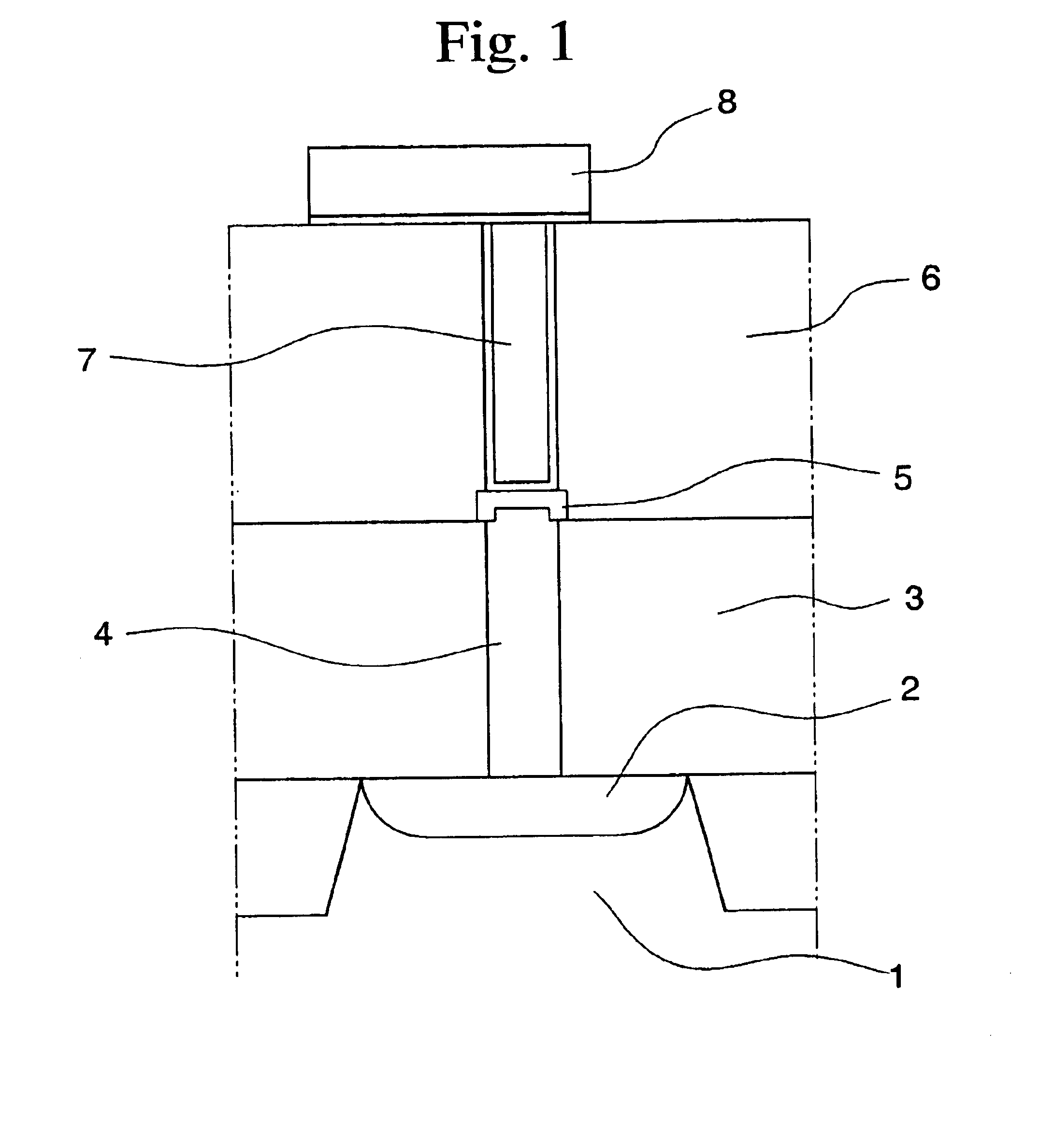
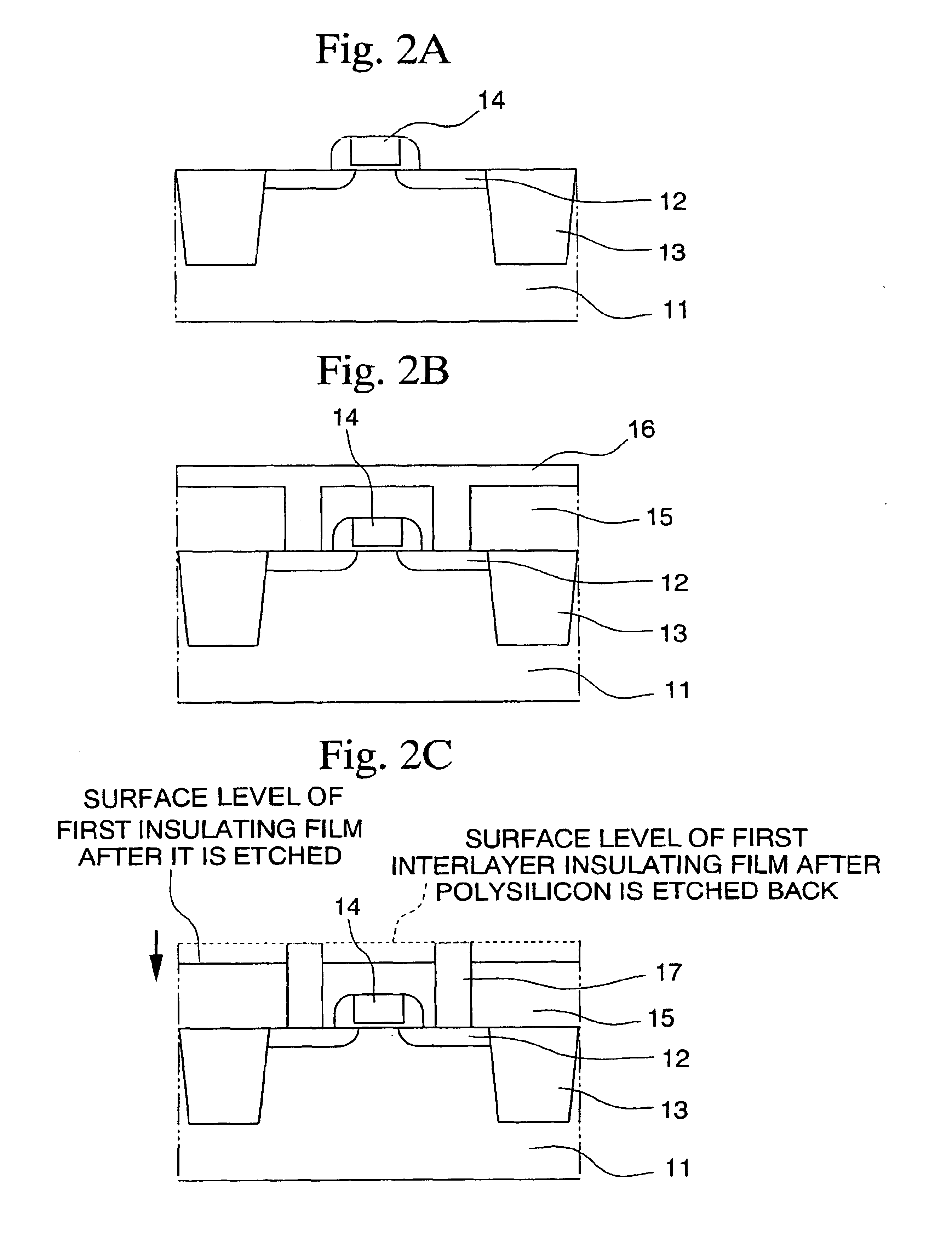
[0041]Hereinafter, several embodiments of the present invention are described with reference to the attached drawings. FIG. 1 is a cross-sectional view showing a structure of a semiconductor device according to the present invention. Here, only the portion relevant to the present invention in the integrated circuit formed on the semiconductor substrate will be explained in order to simplify the explanation.

[0042]As shown in FIG. 1, a silicon oxide film selectively formed for element separation and an n-type high concentration diffusion layer 2, doped with a high concentration N-type impurity, are formed on a P-type silicon substrate 1. On the element separated surface, a silicon oxide film (CVD oxide film) or BPSG (Boro-Phospho-Silicate-Glass) film are arranged as the first interlayer insulating film 3. The film thickness is within a range of from 500 nm to 1.5 μm. In the present embodiment, a film thickness of 500 nm is adopted.

[0043]On the n-type high concentration diffusion layer...

second embodiment

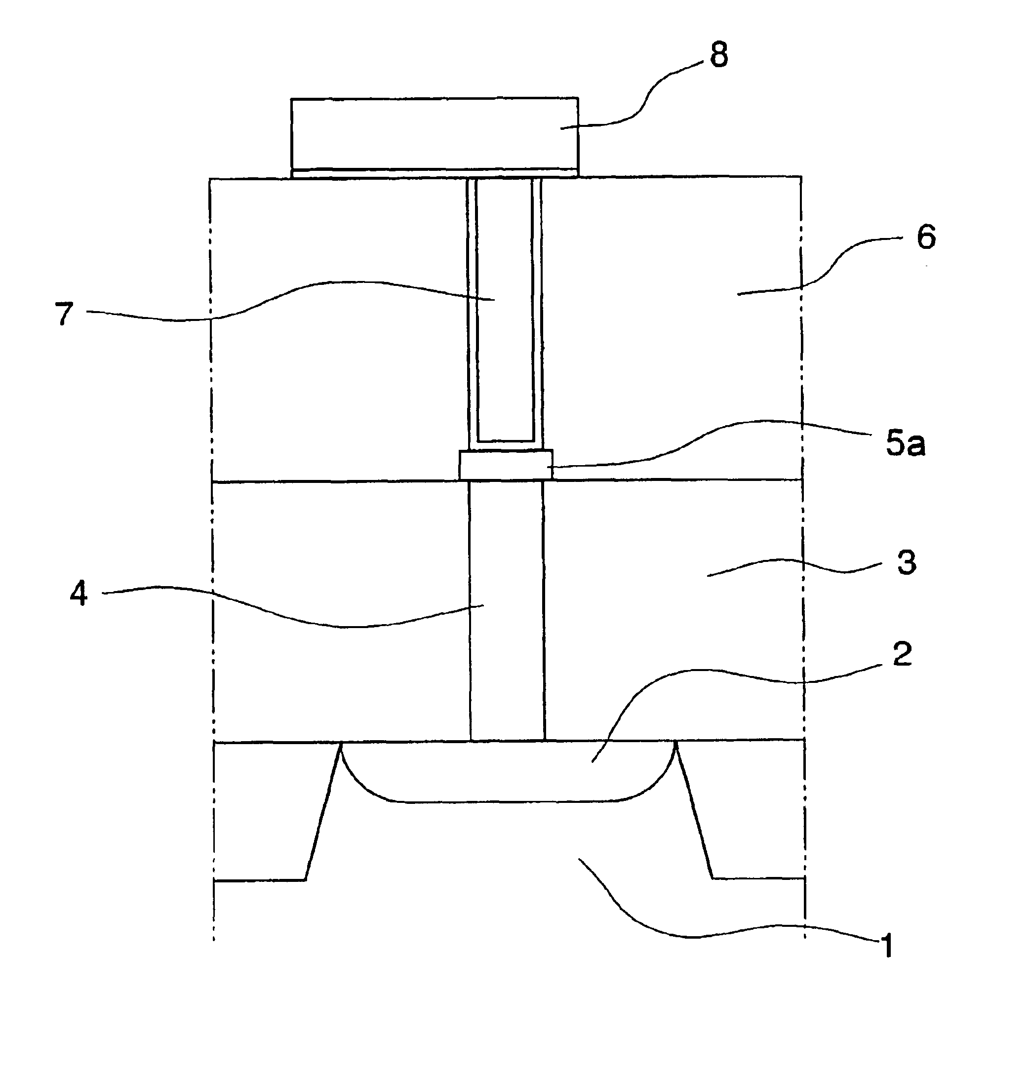
[0067]FIG. 4 is a cross-sectional view showing the structure of the semiconductor device according to the present invention. As shown in FIG. 4, a structural example is shown, in which a silicide pad 5a for connecting the silicon plug 4 and a tungsten plug 7 is not formed in a U-shape.

[0068]That is, as shown in FIG. 4, the silicide pad 5a on the upper end of the polysilicon plug 4 is not necessarily formed in a U-shape. The interface between the polysilicon plug 4 and the silicide pad 5a may be located on the same level as the upper plane of the first interlayer insulating film 3 or below. In this case, it is a feature of the present invention that the outside area of the silicide pad extending from the silicon plug is symmetrical about the center of the silicon plug. In the conventional devices shown in FIG. 5, the silicide pad is not positioned in a self-aligning manner, the silicide pads shifts within the range of mechanical error. That is, when viewed in the cross-sectional dire...


PUM


Abstract

The present invention provides a structure for a semiconductor device, capable of eliminating the generation of defective products due to poor connection. In the present semiconductor device, an n-type high concentration diffusion layer 2 is selectively formed on the P-type silicon substrate 1, and on the diffusion layer 2, a silicon oxide film 3 is formed as a first interlayer insulating film 3. A silicon plug 4 is disposed on the n-type high concentration diffusion layer 2. On the top end surface of the polysilicon plug 4, a silicide pad 5 is formed in a self-aligning manner such that the width of the silicide pad 5 is larger than that of the polysilicon plug 4. A second interlayer insulating film is formed so as to cover the first interlayer insulating film 3 and the silicide pad 5, and a tungsten plug 7 is disposed on the silicide pad 5. On the second interlayer insulating film, wiring 8, made of an aluminum-copper alloy and connected to the tungsten plug, is formed.

Description

BACKGROUND OF THE INVENTION[0001]1. Field of the Invention[0002]The present invention relates to a semiconductor device structure and method of manufacturing the same, and in particular relates to a structure of a silicon LSI (Large Scale Integrated) circuit and a method for manufacturing the same.[0003]2. Background Art[0004]Conventionally, performance and function of the silicon LSI circuit have been improved by contracting the design rule step by step based on scaling in computer graphics. In order to improve yields in the manufacturing process of the silicon LSI circuits, it is indispensable to improve the technique of forming wiring and contacts for connecting elements.[0005]In manufacturing a silicon LSI circuit, a plurality of elements such as MOSFETs (Metal Oxide Semiconductor Field Effect Transistors), which are selectively arranged on the silicon substrate, are connected using contact plugs for wiring for forming a desired electronic circuit.[0006]Furthermore, in order to ...

Claims


Application Information

Patent Timeline
Patent Type & Authority Patents(United States)
IPC IPC(8): H01L21/70H01L21/02H01L21/768H01L21/3205H01L21/8242H01L23/522H01L21/28
CPCH01L21/32053H01L21/76895H01L27/10855H01L27/10888H01L2924/0002H01L2924/00H10B12/0335H10B12/485H01L21/28
Inventor MATSUKI, TAKEOTAKAISHI, YOSHIHIRO
Owner NEC ELECTRONICS CORP
Why Eureka
Try Eureka